Semiconductors are materials whose electrical conductivity can be controlled between that of conductors and insulators. Silicon is the most widely used semiconductor material, but germanium, silicon carbide, gallium nitride, gallium arsenide, and other compounds are also important. By controlling electrons and holes through doping and device structures, semiconductors can switch, amplify, store, sense, and process electrical signals.
This guide explains what are semiconductors, what they are made of, how they work, the main types of semiconductors, semiconductor diodes and transistors, how chips are manufactured, and what semiconductors are used for.
What Are Semiconductors?
Semiconductors are materials whose electrical conductivity can be intentionally controlled, allowing them to behave more like conductors under some conditions and more like insulators under others. This controllable behavior makes them the foundation of diodes, transistors, integrated circuits, processors, memory chips, sensors, and power electronics.
A simple semiconductor definition therefore has two meanings. In physics, a semiconductor is a material with electrical characteristics between a conductor and an insulator. In everyday electronics, the word is also commonly used to describe semiconductor devices and integrated circuits made from those materials.
Silicon dominates modern semiconductor manufacturing because it is abundant, thermally stable, and can form a high-quality oxide layer that is extremely useful in transistor fabrication. McKinsey notes that silicon represents roughly 28% of Earth’s crust, making the raw element widely available even though semiconductor-grade silicon requires exceptional purification.
Why Are They Called Semiconductors?
They are called semiconductors because their electrical conductivity lies between highly conductive materials such as copper and highly resistive materials such as glass or rubber.
Rapidus gives a broad resistivity range of approximately 10−410^{-4} to 108 Ω⋅cm10^8\ \Omega\cdot cm for semiconductor materials, between the approximate ranges associated with good conductors and insulating materials. More importantly, semiconductor conductivity can be deliberately changed by doping, temperature, electric fields, and light.
This controllability is more important than simply having “medium” conductivity. Engineers can create regions that conduct differently and combine them into structures that switch current on and off at extremely high speed.
Key Properties Of Semiconductors
The key properties of semiconductors are controllable conductivity, sensitivity to doping and temperature, defined energy-band behavior, and the ability to form junctions that regulate electrical current.
Important semiconductor characteristics include:
- Conductivity between that of conductors and insulators
- Conductivity that changes through controlled doping
- Electrons and holes acting as charge carriers
- Ability to form P-type and N-type regions
- Formation of P-N junctions
- Fast electrical switching
- Compatibility with highly integrated circuits
- Ability to respond to light, heat, voltage, and electric fields
- Support for signal processing, amplification, sensing, storage, and power control
These properties allow a microscopic semiconductor structure to perform functions that would be impossible with a simple metal conductor.
A Brief History Of Semiconductor Technology
Modern semiconductor technology developed from research into electrical conduction and solid-state materials, then accelerated dramatically after the invention of the transistor in the twentieth century.
Early electronics depended heavily on vacuum tubes. Transistors offered a much smaller, lower-power, and more reliable way to switch and amplify electrical signals. The later development of integrated circuits allowed many transistors and interconnections to be manufactured on the same semiconductor substrate.
Today, advanced chips contain enormous numbers of transistor switches. Intel describes modern semiconductor chips as multilayer structures in which billions of microscopic transistors can work together to perform calculations and store or move information.
How Do Semiconductors Work?
Semiconductors work by controlling the movement of electrical charge carriers—mainly electrons and holes—through a crystal structure. Engineers modify this behavior through doping and combine P-type and N-type regions to create junctions that can switch, rectify, amplify, sense, or process electrical signals.
Conductors Vs Semiconductors Vs Insulators
Conductors, semiconductors, and insulators differ mainly in how easily electrical charge can move through them.
| Material Class | Electrical Behavior | Common Examples | Typical Role |
| Conductors | Current flows easily | Copper, silver, aluminum | Wiring and contacts |
| Semiconductors | Conductivity can be controlled | Silicon, germanium, GaAs, SiC | Switching and signal control |
| Insulators | Strongly resist current | Glass, rubber, ceramics | Electrical isolation |
A metal conductor normally has many mobile electrons available for current flow. An insulator strongly restricts electron movement. A semiconductor occupies the useful middle ground where conductivity can be engineered.
How Electrical Conductivity Works In Semiconductors
Electrical conductivity in semiconductors occurs when charge carriers gain the ability to move through the crystal lattice.
In silicon, electrons normally participate in covalent bonds between atoms. If sufficient thermal or electrical energy is supplied, some electrons can enter a conductive state and move through the material.
When an electron leaves its original position, it also creates a vacancy called a hole. Both the moving electron and the effective movement of the hole contribute to electrical conduction.
Energy Bands And Charge Carriers
Energy bands determine whether electrons can move freely enough to conduct electricity.
The two most important bands are the valence band and conduction band. Electrons in the valence band are generally associated with atomic bonding, while electrons that reach the conduction band can move more freely and contribute to current.
The energy region separating them is called the band gap. Materials such as silicon, silicon carbide, and gallium nitride have different band-gap values, which strongly influence voltage capability, temperature behavior, switching speed, and suitable applications.
What Is Semiconductor Doping?
Semiconductor doping is the controlled introduction of small quantities of impurity atoms into a pure semiconductor to change its electrical conductivity.
For silicon, adding atoms with more usable valence electrons can create N-type material with additional free electrons. Adding atoms with fewer valence electrons can create P-type material with additional holes.
IBM and Rapidus describe doping as the fundamental mechanism used to intentionally alter semiconductor conductivity and create N-type and P-type regions.
How Temperature And Impurities Affect Conductivity
Temperature and impurities affect semiconductor conductivity because both influence the number and mobility of available charge carriers.
As temperature rises, additional electrons may gain enough energy to participate in conduction. This is different from normal metal behavior, where increasing temperature generally increases electrical resistance.
Intentional impurities have an even more powerful effect. Controlled dopant concentrations allow engineers to create precisely defined conductive regions that become the foundation of diodes, transistors, and integrated circuits.
What Are Semiconductors Made Of?
Semiconductors are made from carefully purified elemental or compound materials, with silicon being the dominant material in conventional chips. Other important semiconductor materials include germanium, silicon carbide, gallium nitride, gallium arsenide, and indium phosphide.
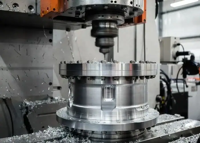
Searching the semiconductor periodic table can sometimes create the impression that all semiconductor materials are individual elements. That is not correct. Some are elemental semiconductors, while others are compounds made by combining elements from different groups.
Similarly, the question “are semiconductors metalloids?” has no universal yes-or-no answer. Silicon and germanium are commonly classified as metalloids, but many important semiconductors, such as GaN, GaAs, and SiC, are compound materials rather than individual metalloids.
| Semiconductor Material | Type | Approx. Band Gap | Typical Applications |
| Silicon | Elemental | 1.12eV | CPUs, memory, ICs, sensors |
| Germanium | Elemental | 0.66eV | Specialized electronics, photonics |
| Silicon Carbide | Compound | ~2.3–3.3eV depending on polytype | EVs, power electronics |
| Gallium Nitride | Compound | ~3.4eV | RF, power electronics, LEDs |
| Gallium Arsenide | Compound | ~1.42eV | RF, optoelectronics |
| Indium Phosphide | Compound | ~1.35eV | Optical communications, photonics |
Silicon
Silicon is the most widely used semiconductor material because it combines controllable electrical properties, thermal stability, abundance, mature manufacturing technology, and excellent compatibility with silicon dioxide.
Semiconductor manufacturing does not use ordinary industrial silicon directly. Electronic-grade material requires extremely high purity before it is converted into wafers.
Intel notes that modern silicon wafers can use silicon purity from about 6N to 9N, corresponding to 99.9999% to 99.9999999% purity.
Germanium
Germanium is an elemental semiconductor with high carrier mobility and a relatively small band gap, but it is used much less widely than silicon in mainstream integrated circuits.
Germanium played an important role in early transistor technology and remains useful in specialized semiconductor structures, photodetectors, infrared systems, and silicon-germanium devices.
Its lower band gap can provide useful electrical behavior but also increases leakage concerns at higher temperatures.
Compound Semiconductors
Compound semiconductors are materials formed from two or more elements that provide properties not available from conventional silicon alone.
Common semiconductors examples include gallium arsenide, gallium nitride, silicon carbide, and indium phosphide.
These materials are especially important when applications require high frequency, optical emission, high voltage, high temperature, or very efficient power conversion.
Silicon Carbide And Wide-Bandgap Materials
Silicon carbide and gallium nitride are wide-bandgap semiconductor materials designed for applications where conventional silicon approaches electrical, thermal, or switching limitations.
Their larger band gaps enable devices to operate at higher electric fields and, depending on device design, at higher temperatures or switching frequencies.
This makes wide-bandgap semiconductors particularly important in electric vehicles, charging systems, renewable-energy conversion, industrial power systems, and high-efficiency power supplies.
Silicon Vs Silicon Carbide
Silicon is usually better for mainstream integrated circuits and cost-sensitive electronics, while silicon carbide is especially attractive for high-voltage and high-power applications.
| Factor | Silicon | Silicon Carbide |
| Manufacturing maturity | Very high | Growing |
| Material cost | Lower | Higher |
| Band gap | ~1.12eV | Much wider |
| High-voltage capability | Good | Better |
| High-temperature operation | More limited | Better |
| Power switching losses | Higher in demanding applications | Often lower |
| Common use | CPUs, memory, ICs | EV inverters, chargers, power modules |
McKinsey highlights SiC and GaN as important materials for high-power and high-frequency applications because they can reduce energy losses and enable smaller system designs.
What Are The Main Types Of Semiconductors?
The main types of semiconductors are intrinsic and extrinsic semiconductors, with extrinsic materials further divided into N-type and P-type semiconductors. Semiconductors can also be classified by composition as elemental or compound materials and by band-gap characteristics.
These classifications describe different things. “Intrinsic versus extrinsic” describes whether the material has been intentionally doped, while “N-type versus P-type” describes the dominant charge carrier created through doping.
“Elemental versus compound” describes chemical composition.
Intrinsic Semiconductors
An intrinsic semiconductor is a semiconductor material in a highly pure, intentionally undoped state.
In an ideal intrinsic material, thermally generated electrons and holes occur in equal concentrations. Silicon and germanium can both behave as intrinsic semiconductors when sufficiently pure.
Intrinsic semiconductor behavior provides the foundation for understanding how deliberately introduced dopants change electrical conductivity.
Extrinsic Semiconductors
Extrinsic semiconductors are semiconductor materials whose electrical properties have been intentionally modified through doping.
The controlled impurities increase the concentration of either electrons or holes, allowing conductivity to be adjusted for a specific device function.
Nearly all practical silicon electronic devices rely on carefully controlled extrinsic regions rather than using purely intrinsic material throughout the device.
N-Type Semiconductors
N-type semiconductors are doped semiconductor materials in which electrons are the majority charge carriers.
For silicon, dopants such as phosphorus, arsenic, or antimony can contribute additional electrons. These dopant atoms are commonly called donors because they donate electrons that can participate in conduction.
Holes still exist in N-type material, but they are minority carriers.
P-Type Semiconductors
P-type semiconductors are doped semiconductor materials in which holes are the majority charge carriers.
Boron and similar acceptor dopants have fewer valence electrons than silicon. Their presence creates electron vacancies that behave electrically as positive charge carriers.
Electrons remain present, but holes dominate the conduction behavior of the P-type region.
Elemental And Compound Semiconductors
Elemental semiconductors consist primarily of one chemical element, while compound semiconductors combine two or more elements.
Silicon and germanium are familiar elemental examples. Gallium arsenide, silicon carbide, gallium nitride, and indium phosphide are compound semiconductors.
The choice depends on electrical performance, thermal requirements, frequency, optical behavior, voltage, manufacturing maturity, and cost.
How Do P-Type And N-Type Semiconductors Work Together?
P-type and N-type semiconductors work together by forming a P-N junction, where electrons and holes interact to create a depletion region that can control the direction and amount of electrical current. This structure is the foundation of semiconductor diodes and many transistor designs.
Electrons And Holes As Charge Carriers
Electrons and holes are the two primary charge carriers responsible for current flow in semiconductor materials.
Electrons carry negative charge. A hole represents the absence of an electron in a bond and behaves as an effective positive charge as neighboring electrons move to fill vacancies.
N-type material contains more mobile electrons, while P-type material contains more holes.
How P-N Junctions Form
A P-N junction forms when P-type and N-type semiconductor regions are placed next to each other within the same semiconductor structure.
Near the boundary, electrons diffuse from the N-type side and recombine with holes from the P-type side. This process leaves behind fixed charged ions and produces a carrier-depleted region.
That depletion region creates an internal electric field and potential barrier.
How A P-N Junction Controls Current
A P-N junction controls current by changing its electrical barrier according to the direction of the applied voltage.
Under forward bias, the barrier becomes easier for carriers to cross and substantial current can flow. Under reverse bias, the depletion region expands and strongly restricts current under normal operating conditions.
This one-direction behavior forms the basic operating principle of a semiconductor diode.
What Are The Main Semiconductor Devices?
The main semiconductor devices include diodes, transistors, integrated circuits, processors, memory devices, sensors, and power semiconductors. Each uses controlled semiconductor regions to perform functions such as switching, amplification, computation, storage, sensing, rectification, or power conversion.
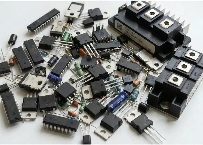
Semiconductor Diodes
A semiconductor diode is a device designed primarily to allow current to flow more easily in one direction than the other.
Basic diodes use a P-N junction. Variations include rectifier diodes, Zener diodes, photodiodes, laser diodes, and light-emitting diodes.
Applications range from AC-to-DC power conversion and voltage protection to optical sensing and lighting.
Transistors
Transistors are semiconductor devices used primarily for switching or amplifying electrical signals.
In digital electronics, transistors act like extremely fast microscopic switches. Large numbers of them can represent and manipulate binary information.
Rapidus describes this switching behavior as the basis for digital calculation, while Intel notes that modern semiconductor devices can contain billions of microscopic transistor switches.
Integrated Circuits And Semiconductor Chips
Integrated circuits are semiconductor chips that combine many electrical components and interconnections on a small semiconductor die.
Depending on their purpose, chips may contain transistors, diodes, memory cells, analog circuits, power-control structures, communication circuits, and other components.
Modern ICs range from very simple controllers to advanced CPUs, GPUs, memory devices, and AI accelerators.
Power Semiconductor Devices
Power semiconductor devices control or convert relatively high voltages and currents in systems such as electric vehicles, industrial drives, chargers, power supplies, solar inverters, and energy infrastructure.
Typical devices include power MOSFETs, IGBTs, power diodes, and wide-bandgap SiC or GaN devices.
Their engineering priority is usually efficient conversion with low switching and conduction losses.
Processors And Major Processor Architectures
Processor architectures differ according to how semiconductor circuits are optimized for computing workloads.
| Architecture | Main Function | Common Applications |
| CPU | General-purpose sequential computing | PCs, servers, control systems |
| GPU | Highly parallel computation | Graphics, AI, scientific computing |
| FPGA | Reconfigurable hardware logic | Prototyping, communications, acceleration |
| ASIC | Dedicated application-specific processing | AI, networking, encryption, custom systems |
Intel identifies CPUs, GPUs, FPGAs, and ASICs as major processor categories, each optimized for different workloads.
How Are Semiconductors And Chips Manufactured?
Semiconductors and chips are manufactured by purifying semiconductor material, creating wafers, repeatedly forming microscopic patterned layers through processes such as lithography, deposition, doping, and etching, testing the completed wafer, cutting it into dies, and packaging the functional dies into finished semiconductor devices.
Semiconductor manufacturing is one of the most precision-intensive manufacturing systems in industry. McKinsey notes that fabrication requires nanometer-scale precision, atomic-level control, high chemical purity, and highly coordinated processing across many repeated manufacturing steps.
The simplified flow is:
Raw Material → Crystal → Wafer → Lithography → Deposition / Etching / Doping → Interconnects → Wafer Test → Dicing → Packaging → Final Test
Semiconductor Material Preparation
Semiconductor material preparation begins with obtaining an extremely pure material with tightly controlled electrical and structural properties.
For conventional silicon chips, raw silicon is refined and purified before single-crystal material is produced.
Contamination that would be insignificant in ordinary manufacturing can dramatically affect semiconductor electrical behavior, making purity and contamination control critical.
Wafer Production
Wafer production converts high-purity semiconductor crystal into thin circular substrates used for device fabrication.
Modern high-volume silicon manufacturing commonly uses 300mm wafers. Intel describes its modern wafers as approximately 300mm in diameter and about 0.775mm thick.
The wafer must meet demanding requirements for flatness, surface quality, crystal orientation, purity, and defect control.
What Is Wafer Fabrication?
Wafer fabrication is the repeated process of building microscopic semiconductor structures and interconnections on the surface of a wafer.
A wafer passes through many operations, and certain types of equipment may be revisited repeatedly as new device layers are created.
McKinsey describes fabs as complex facilities involving hundreds of sequential operations and thousands of repeatedly used equipment chambers and data streams.
Masking And Photolithography
Photolithography transfers microscopic circuit patterns from a mask onto a light-sensitive coating applied to the wafer.
Light exposes selected areas of photoresist according to the circuit pattern. Chemical development then creates patterned regions that guide subsequent processing.
Multiple masks are required because an advanced chip contains many different functional and interconnection layers.
Doping, Deposition, Etching, And Layer Formation
Doping, deposition, and etching create the electrically active regions and physical structures required for semiconductor devices.
Doping changes electrical behavior by introducing selected atoms. Deposition adds thin layers of materials. Etching selectively removes material according to patterned masks.
These operations are repeated many times until transistors, contacts, insulating layers, and metal interconnections form the intended circuit.
Wafer Testing And Die Sorting
Wafer testing identifies which individual circuits on a completed wafer meet electrical and functional requirements.
Probe systems make temporary electrical contact with individual dies and perform defined tests before packaging.
Known defective dies can then be excluded from further processing, reducing the cost of packaging components that would later fail.
Semiconductor Packaging And Assembly
Semiconductor packaging protects the delicate die while providing mechanical support, electrical connections, and thermal paths to the final system.
After the wafer is separated into individual dies, one or more dies can be attached to a substrate or package and interconnected.
Advanced packaging can combine multiple chiplets, memory, logic, and other components inside increasingly sophisticated package architectures.
Final Testing And Distribution
Final testing verifies packaged semiconductor devices before they are released into the supply chain.
Testing may evaluate electrical function, speed, power consumption, voltage behavior, thermal response, reliability, and application-specific requirements.
Intel notes that assembly and test can involve hundreds of additional manufacturing operations after wafer fabrication is complete.
What Manufacturing Processes Are Used In The Semiconductor Industry?
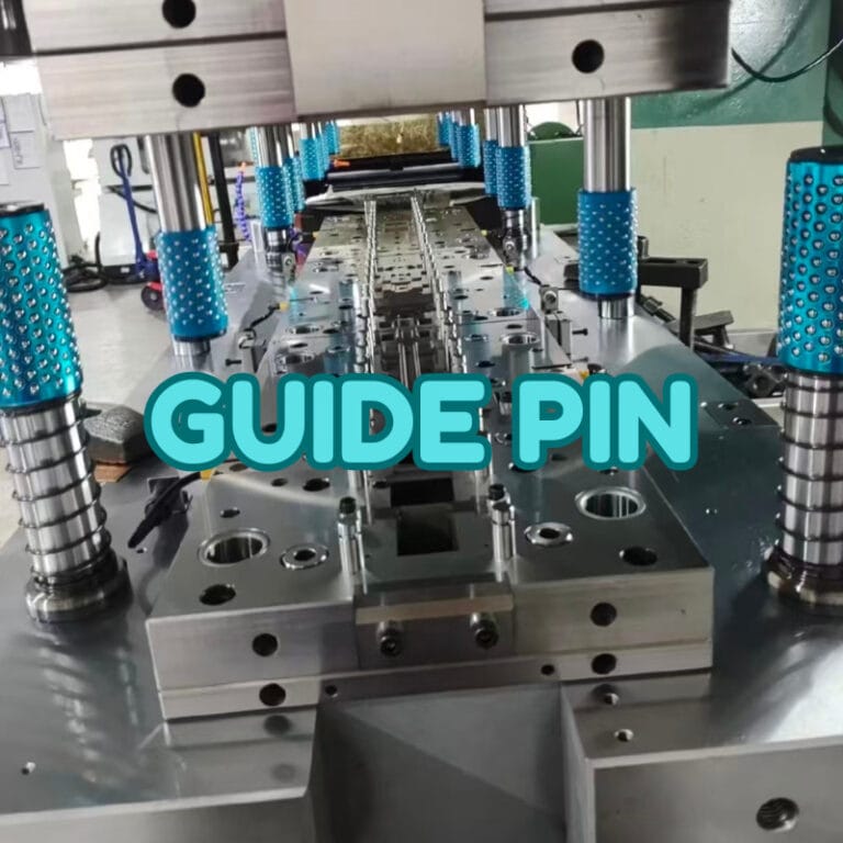
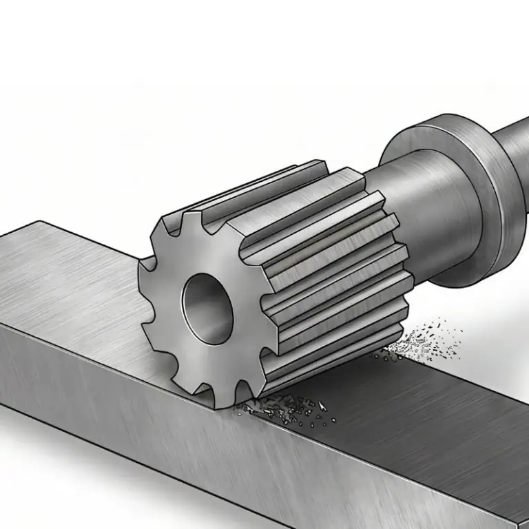
Manufacturing processes used for semiconductor equipment and precision components include CNC machining, sheet metal fabrication, precision grinding, EDM, welding, additive manufacturing, and surface finishing. CNC machining is one of the most widely used processes for producing high-precision mechanical parts, while other processes support thin-sheet structures, hardened tooling, complex features, assemblies, prototypes, and controlled surfaces.
CNC Machining
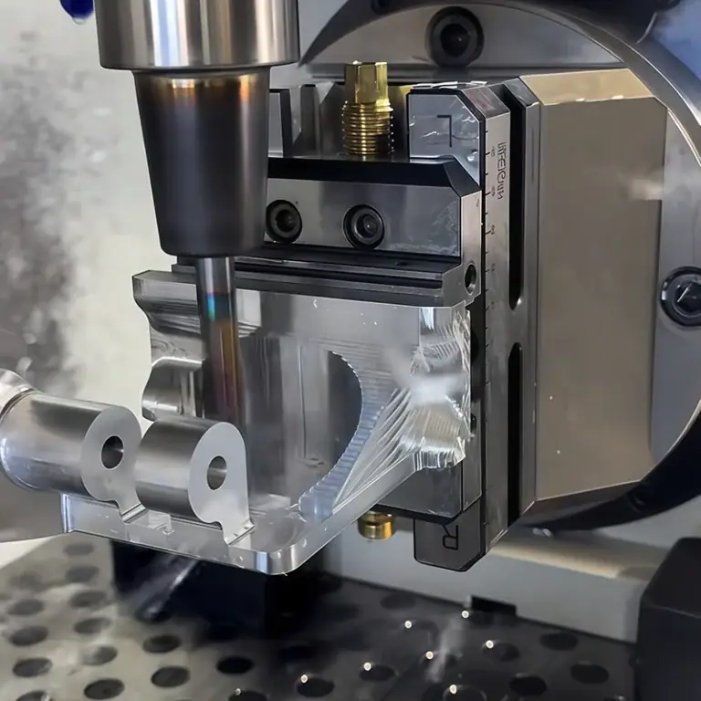
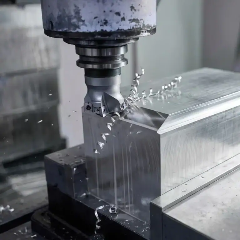
CNC machining is used to manufacture precision semiconductor equipment components from aluminum, stainless steel, copper, PEEK, PTFE, and other engineering materials.
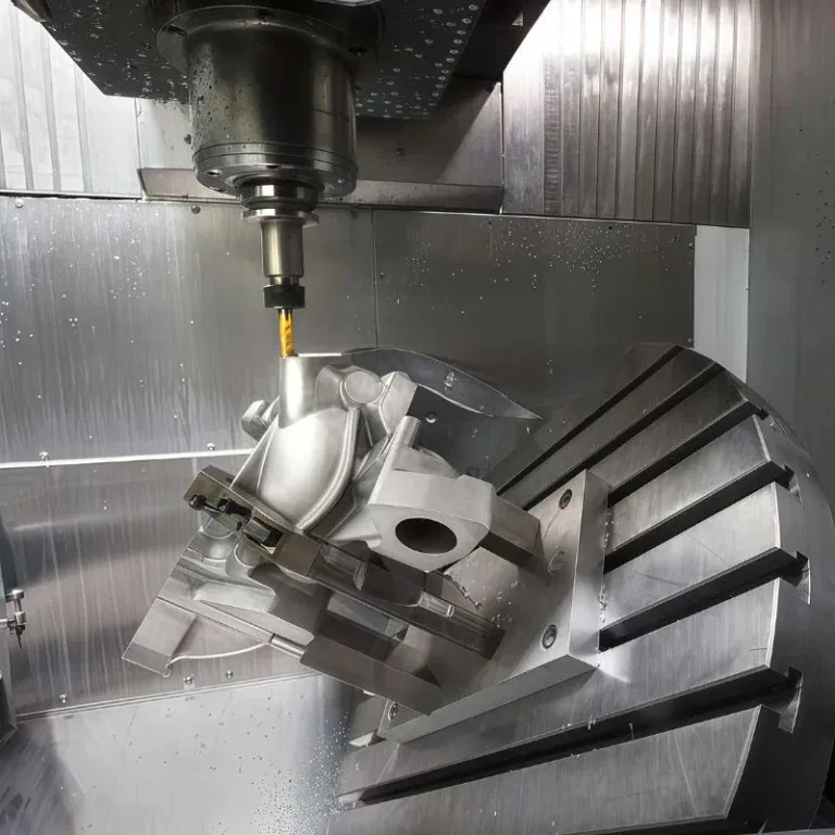
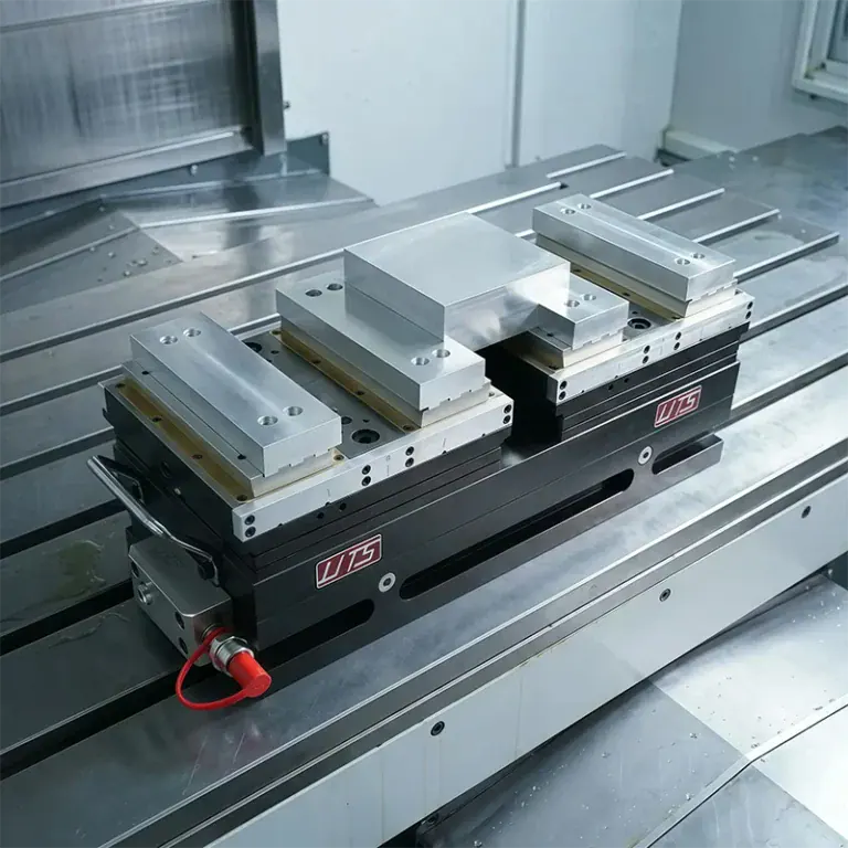
CNC milling, CNC turning, drilling, tapping, and 5-axis machining can be combined depending on part geometry. Typical components include vacuum chamber parts, wafer-handling fixtures, equipment housings, cooling plates, precision bases, sensor mounts, robotic interfaces, and inspection-system components.
For semiconductor applications, dimensional tolerance alone is not enough. Flatness, surface finish, burr control, cleanliness, thermal stability, and contamination control may also need to be specified.
Sheet Metal Fabrication
Sheet metal fabrication is used for semiconductor equipment enclosures, machine covers, electrical cabinets, brackets, guards, internal panels, trays, and structural assemblies.
Common processes include laser cutting, punching, bending, forming, riveting, and hardware insertion. Aluminum and stainless steel are frequently selected because they provide useful combinations of corrosion resistance, cleanliness, weight, and structural performance.
Sheet metal fabrication is especially economical for large, thin-walled parts that would create excessive material waste if machined entirely from solid stock.
Precision Grinding
Precision grinding is used when semiconductor equipment components require very tight flatness, parallelism, dimensional accuracy, or controlled surface finish.
Typical applications include machine bases, precision plates, guide surfaces, tooling components, stages, fixtures, and hardened mechanical parts.
Grinding is often performed after CNC machining. CNC establishes the main geometry, while grinding brings selected reference or mating surfaces to tighter final tolerances.
EDM
EDM is used to manufacture conductive components with deep, narrow, sharp, or difficult-to-access features that conventional cutting tools cannot produce efficiently.
Wire EDM is suitable for precision profiles, narrow slots, inserts, electrodes, tooling, and hardened parts. Sinker EDM is useful for cavities and complex internal geometry.
In semiconductor equipment manufacturing, EDM is normally used together with CNC machining rather than as the main process for every component.
Welding And Fabrication
Welding and fabrication are used to build larger semiconductor equipment structures, frames, vacuum-related assemblies, stainless steel systems, supports, and machine components.
TIG welding is particularly common for stainless steel and aluminum assemblies where clean welds and good process control are required.
For precision equipment, welding sequence, heat input, distortion, fixture design, and post-weld machining must be controlled because thermal deformation can affect flatness and assembly accuracy.
Additive Manufacturing
Additive manufacturing is used mainly for semiconductor equipment prototypes, development parts, complex internal channels, lightweight structures, and low-volume components.
Metal 3D printing can create geometries that are difficult to machine conventionally, while polymer 3D printing is useful for fixtures, covers, handling aids, and prototype components.
However, dimensional tolerance and surface finish are usually lower than precision CNC machining, so critical interfaces may require secondary machining.
Surface Finishing
Surface finishing is used to improve corrosion resistance, cleanliness, wear resistance, appearance, electrical behavior, or surface performance of semiconductor equipment components.
Common treatments include:
- Anodizing
- Electroless nickel plating
- Passivation
- Polishing
- Electropolishing
- Bead blasting
- Chemical cleaning
- Precision cleaning
The correct finish depends on the component location and operating environment. Vacuum components, chemical-handling parts, optical systems, and external equipment covers can require very different surface specifications.
Precision Cleaning
Precision cleaning is especially important for semiconductor equipment components because particles, machining oils, burrs, residues, and surface contamination can affect sensitive manufacturing environments.
Cleaning may include ultrasonic cleaning, aqueous cleaning, solvent cleaning, deionized-water rinsing, controlled drying, and clean packaging.
For semiconductor equipment, the complete manufacturing route can therefore be:
CNC Machining → Sheet Metal / Grinding / EDM / Welding As Required → Surface Finishing → Precision Cleaning → Dimensional Inspection → Clean Packaging
What Are The Advantages Of Semiconductors?
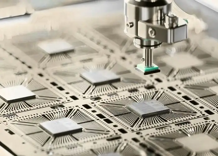
The main advantages of semiconductors are controllable conductivity, extremely small device size, high switching speed, low energy consumption, high integration density, reliability, scalability, and the ability to perform many different electrical functions on compact chips.
Controlled Electrical Conductivity
Controlled conductivity allows semiconductor devices to switch, direct, amplify, and regulate electrical signals.
Unlike ordinary conductors, their electrical behavior can be engineered through doping, junction design, electric fields, and device geometry.
That controllability is the fundamental reason digital logic can exist.
Small Size And High Integration
Semiconductors allow enormous numbers of electrical devices to be integrated onto a very small area.
A single modern chip can combine processing, cache, memory interfaces, communication circuits, and billions of transistors.
High integration reduces system size while increasing functionality.
Fast Switching And Processing
Semiconductor devices can switch at extremely high speeds, enabling modern processors to execute enormous numbers of operations every second.
Fast switching supports real-time computing, high-speed networking, AI inference, image processing, industrial control, and communications.
Performance depends on architecture as well as the underlying transistor technology.
Energy Efficiency
Semiconductor technology improves energy efficiency by controlling electrical power with increasingly low switching and conduction losses.
Efficiency is especially important in battery-powered electronics, data centers, electric vehicles, renewable-energy conversion, and industrial motor drives.
Wide-bandgap semiconductor materials can provide additional efficiency advantages in demanding high-voltage applications.
Reliability And Scalability
Semiconductors provide high reliability and scalable manufacturing when designs and production processes are properly controlled.
The same wafer fabrication process can produce many dies across each wafer, while repeatable manufacturing allows semiconductor products to reach very large production quantities.
Rigorous electrical, mechanical, thermal, and reliability testing supports use in demanding applications ranging from servers to transportation and medical equipment.
What Are Semiconductors Used For?
Semiconductors are used for computing, data storage, communications, sensing, power conversion, motor control, automotive systems, medical equipment, industrial automation, consumer electronics, artificial intelligence, and nearly every modern electronic system.
Computing And Data Centers
Semiconductors are used in computing and data centers as CPUs, GPUs, memory, storage controllers, networking processors, power-management ICs, and specialized accelerators.
AI infrastructure has increased demand for high-performance processors, high-bandwidth memory, networking components, and power-control devices.
Gartner reported that AI-related semiconductor categories accounted for nearly one-third of semiconductor sales in 2025.
Consumer Electronics And IoT
Semiconductors are used in consumer electronics and IoT devices to process data, connect networks, control displays, measure sensors, manage batteries, and operate motors.
Smartphones, laptops, televisions, cameras, watches, appliances, home-control devices, gaming systems, and wearable electronics all depend on semiconductor components.
Many apparently simple connected devices contain several different chip types.
Communications
Semiconductors are used in communications equipment to generate, transmit, receive, convert, and process digital and radio-frequency signals.
Applications include smartphones, base stations, routers, optical networks, satellite systems, Wi-Fi equipment, radios, and data-center networking.
High-frequency materials such as GaAs and GaN are particularly useful in selected RF applications.
Automotive And Transportation
Semiconductors are used in vehicles for powertrain control, battery management, infotainment, safety systems, sensors, lighting, communications, and advanced driver-assistance systems.
Electric vehicles require additional power-semiconductor content for battery charging, inverters, DC-DC conversion, and motor control.
Silicon carbide has become especially valuable in high-voltage EV power electronics because of its efficiency advantages.
Medical And Healthcare Devices
Semiconductors are used in medical equipment for sensing, imaging, signal processing, monitoring, communication, and precise electronic control.
Intel lists examples such as blood-pressure sensors, hearing aids, MRI equipment, pacemakers, ultrasound modules, and wireless patient-monitoring systems.
Reliability, traceability, power consumption, and signal integrity can be especially important in medical applications.
Smart Manufacturing And Industrial Automation
Semiconductors are used in smart manufacturing for machine control, robotics, PLCs, servo drives, vision systems, sensors, industrial networking, predictive maintenance, and automated inspection.
Automation systems require processors to make decisions, memory to store programs, sensors to collect physical data, and power devices to control motors and actuators.
Semiconductor manufacturing equipment itself also depends on precision motion control, vacuum systems, optics, robotics, thermal control, and tightly toleranced mechanical assemblies.
Smart Energy And Power Electronics
Semiconductors are used in energy systems to switch, regulate, convert, measure, and distribute electrical power efficiently.
Solar inverters, wind-power systems, battery-storage systems, EV chargers, smart grids, motor drives, and high-efficiency power supplies all use semiconductor power devices.
SiC and GaN are increasingly important where higher switching efficiency can reduce heat, component size, or electrical losses.
Artificial Intelligence And Advanced Computing
Semiconductors are used in AI to perform the enormous matrix, vector, memory, networking, and data-transfer workloads required to train and run machine-learning models.
GPUs, custom ASICs, CPUs, memory, networking chips, and power-management devices all contribute to an AI computing platform.
AI therefore depends on much more than a single “AI chip”, it requires a complete semiconductor ecosystem.
How Do Semiconductors Drive Modern Innovation?
Semiconductors drive modern innovation by making computing faster, electronics smaller, power systems more efficient, machines more intelligent, and communication systems more capable. Improvements in semiconductor devices frequently enable improvements across entire industries.
Artificial Intelligence
Semiconductors drive AI by supplying the computation, memory bandwidth, networking, storage, and power-management capability required for modern models.
GPUs and AI ASICs perform huge numbers of parallel calculations, while high-bandwidth memory reduces data-transfer bottlenecks.
Increasing AI model size therefore creates demand throughout the semiconductor stack rather than only for processors.
Electric Vehicles And Autonomous Systems
Semiconductors drive electric vehicles through power conversion, sensing, battery control, motor control, computing, safety systems, and communications.
Autonomous and advanced-driver-assistance functions further increase requirements for cameras, radar, processors, memory, and sensor interfaces.
Higher vehicle electrification generally means greater semiconductor content per vehicle.
5G And Advanced Communications
Semiconductors enable advanced communications by generating and processing high-frequency signals while performing increasingly complex digital signal processing.
RF front ends, modem chips, network processors, analog devices, power amplifiers, and optical components all contribute to modern communication systems.
Specialized materials may be selected when conventional silicon cannot efficiently meet frequency or power requirements.
Industrial Automation And Robotics
Semiconductors enable automation and robotics by connecting sensing, computation, communication, and motion control.
A robotic system may use processors for path planning, sensors for position and vision, memory for software, network ICs for communication, and power semiconductors for servo-motor control.
Better semiconductor performance can therefore produce faster and more energy-efficient automated equipment.
Healthcare Technology
Semiconductors enable healthcare technology by allowing medical systems to sense weak signals, process images, control devices, store data, and communicate wirelessly.
Diagnostic imaging, portable monitoring, hearing devices, laboratory automation, surgical equipment, and wearable sensors all depend on semiconductor electronics.
Miniaturization also allows increasingly capable electronics to be incorporated into smaller medical systems.
Energy And Power Conversion
Semiconductors enable more efficient energy conversion by rapidly switching and regulating electrical power.
Power electronics influence efficiency from electricity generation through distribution and final equipment use.
Reducing semiconductor switching losses can lower heat generation, shrink cooling requirements, and improve the energy efficiency of EVs, renewable-energy systems, chargers, industrial equipment, and data centers.
What Is Semiconductor Engineering?
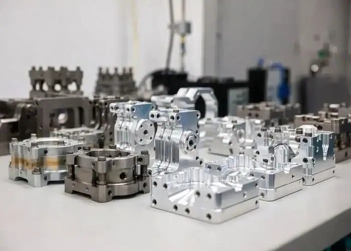
Semiconductor engineering is the multidisciplinary engineering work involved in designing semiconductor devices, developing fabrication processes, manufacturing wafers, packaging and testing chips, and building the highly specialized equipment required for semiconductor production.
Semiconductor Design
Semiconductor design defines the electrical architecture and physical circuit structure that a chip must contain.
Engineers may work on transistor-level circuits, digital logic, analog designs, processor architecture, memory, RF circuits, power management, or physical layout.
Design verification ensures the chip behaves correctly before committing to costly fabrication.
Process And Manufacturing Engineering
Process and manufacturing engineering develops and controls the fabrication steps used to convert a blank wafer into functional semiconductor devices.
Engineers manage deposition, lithography, etching, ion implantation, thermal processing, cleaning, metrology, defect reduction, and yield.
At advanced nodes, process windows become increasingly narrow, making statistical process control and equipment consistency critical.
Packaging And Testing Engineering
Packaging and testing engineering converts fragile semiconductor dies into usable products while verifying their electrical performance.
Packaging engineers manage interconnection density, thermal dissipation, mechanical reliability, substrates, solder joints, chiplets, and advanced integration.
Test engineers identify defective products and characterize performance before components enter final electronic systems.
Equipment And Production Engineering
Equipment and production engineering develops and maintains the machines, fixtures, automation, vacuum systems, motion stages, thermal systems, and precision mechanical assemblies used inside fabs and packaging facilities.
These systems may require precision-machined aluminum, stainless steel, copper, engineering plastics, vacuum-compatible components, fixtures, housings, heat sinks, robotic interfaces, and multi-axis parts.
Because semiconductor tools demand repeatable positioning, cleanliness, thermal stability, and controlled surfaces, mechanical manufacturing quality can directly influence equipment performance.
How Does The Global Semiconductor Supply Chain Work?
The global semiconductor supply chain divides chip development among specialized companies and regions responsible for design, equipment, materials, wafer fabrication, packaging, testing, and final electronics manufacturing. No single country currently performs every stage of the most advanced supply chain independently.
Chip Design And Intellectual Property
Chip design and intellectual property determine what the semiconductor will do before fabrication begins.
Fabless companies may design chips without owning wafer fabrication plants, while integrated device manufacturers combine design with internal manufacturing.
Specialized IP providers also license processor cores, interfaces, and other design technologies.
Wafer Fabrication And Foundries
Wafer foundries manufacture semiconductor designs on behalf of customers using tightly controlled fabrication processes.
TSMC is currently the largest pure-play foundry. TrendForce reported a 70.4% share of global foundry revenue for TSMC in Q4 2025, showing how concentrated advanced wafer fabrication has become.
Foundries differentiate through process nodes, capacity, yield, manufacturing reliability, packaging capability, and technology specialization.
Assembly, Packaging, And Testing
Assembly, packaging, and testing convert fabricated wafers into protected, electrically connected components ready for installation on circuit boards or larger systems.
This stage increasingly contributes to performance because advanced packaging can connect multiple logic, memory, and specialized dies within one system.
High-bandwidth memory and chiplet architectures have made packaging capability particularly strategic.
Regional Semiconductor Manufacturing Specialization
Semiconductor regions specialize in different parts of the value chain rather than competing on exactly the same capability.
The United States has major strengths in semiconductor design, R&D, equipment, and company revenue. Taiwan has extraordinary strength in foundry manufacturing, especially advanced processes. South Korea is particularly strong in memory, while Japan and Europe hold important positions in equipment, materials, automotive semiconductors, sensors, and specialty technologies.
China continues expanding mature-node manufacturing and its broader semiconductor ecosystem.
Why Semiconductor Manufacturing Is A Global Business
Semiconductor manufacturing is global because producing an advanced chip requires expertise, equipment, materials, intellectual property, capital, and manufacturing capacity from many specialized suppliers.
A single fab can require hundreds of types of specialized equipment and highly purified gases, chemicals, metals, substrates, optics, and precision components.
The complexity and investment required make semiconductor supply chains highly interconnected.
What Challenges Does The Semiconductor Industry Face?
The semiconductor industry faces challenges from rapidly growing demand, enormous capital requirements, manufacturing complexity, supply-chain concentration, geopolitical restrictions, skilled-labor shortages, environmental impact, and the technical difficulty of continuing performance improvements.
Rapid Growth In Semiconductor Demand
Semiconductor demand is growing because more products require computing, sensing, connectivity, memory, and power electronics.
AI infrastructure is currently a particularly strong demand driver. Gartner reported worldwide semiconductor revenue of approximately $793billion in 2025, up 21% year over year.
Automotive electronics, industrial automation, data centers, communications, and electrification provide additional demand.
Manufacturing Capacity And Supply Constraints
Manufacturing capacity can become constrained because advanced fabs require huge investment and cannot be created quickly.
Production also depends on specialized equipment, materials, utilities, engineers, and qualified processes.
Increasing nominal wafer capacity does not automatically solve shortages if the required process node, packaging technology, memory type, or product qualification is different.
Semiconductor Shortages And Supply Chain Risk
Semiconductor shortages occur when demand, inventory, manufacturing capacity, logistics, or product mix become misaligned.
The pandemic-era shortage demonstrated that disruptions can affect automotive, consumer electronics, industrial equipment, and many other markets simultaneously.
Long qualification cycles make certain semiconductor products difficult to substitute quickly.
Geopolitical And Trade Risks
Geopolitical and trade risks affect semiconductor access because advanced chips and manufacturing equipment have strategic economic and national-security importance.
Export controls, subsidies, regional manufacturing incentives, tariffs, and technology restrictions increasingly influence company investment decisions.
As a result, manufacturers are investing in additional regional capacity even when global specialization remains economically important.
Advanced Manufacturing Complexity
Advanced semiconductor manufacturing is difficult because enormous numbers of microscopic features must be formed with extremely low defect rates.
Any contamination, overlay error, dimensional variation, process drift, or equipment failure can reduce yield.
McKinsey describes semiconductor fabrication as requiring nanometer-scale precision and high chemical purity across highly iterative production systems.
Energy Use, Water Use, And Emissions
Semiconductor manufacturing requires substantial energy, water, process gases, chemicals, and controlled facility infrastructure.
Advanced fabs use purified water for wafer cleaning and significant electricity for cleanrooms, processing equipment, vacuum systems, cooling, and utilities.
Future manufacturing expansion therefore requires improvements in water recycling, energy efficiency, emissions control, chemical management, and renewable-energy sourcing.
What Is The Future Of Semiconductor Technology?
The future of semiconductor technology will combine smaller and more efficient transistors with advanced materials, chiplets, three-dimensional integration, advanced packaging, AI-specific architectures, power semiconductors, and expanded global manufacturing capacity.
Advanced Semiconductor Materials
Advanced semiconductor materials will expand where silicon cannot provide the required power, frequency, optical, or thermal performance.
SiC and GaN are already growing in power electronics, while materials such as InP remain valuable for optical and high-frequency applications.
Research continues into new semiconductor structures and materials for future computing and energy systems.
Smaller And More Efficient Chips
Future chips will continue pursuing greater computational capability per unit of area and energy.
New transistor architectures, improved lithography, process integration, power delivery, interconnect technologies, and materials can increase transistor density and performance.
Efficiency will be increasingly important because power and cooling are major constraints in advanced computing.
Advanced Semiconductor Packaging
Advanced packaging will become more important as designers combine multiple dies instead of relying entirely on one monolithic chip.
Chiplets, 2.5D structures, 3D stacking, high-density interconnects, and advanced substrates can place logic and memory much closer together.
This approach can improve bandwidth and allow different semiconductor technologies to be combined inside one package.
AI-Focused Semiconductor Architectures
AI-focused semiconductor architectures will continue growing because AI workloads demand very high parallel computing performance and memory bandwidth.
GPUs will remain important, but application-specific AI accelerators, custom silicon, advanced networking chips, and specialized inference processors are also expanding.
The AI hardware ecosystem will therefore become increasingly diverse rather than converging on one processor type.
Growing Demand For Power Semiconductors
Power-semiconductor demand will grow as transportation, energy, data centers, and industrial systems become increasingly electrified.
EV powertrains, charging infrastructure, solar systems, battery storage, industrial drives, and data-center power delivery all require efficient power conversion.
SiC, GaN, and improved silicon power devices will each serve different voltage, frequency, performance, and cost ranges.
Expansion Of Global Manufacturing Capacity
Global semiconductor manufacturing capacity will continue expanding as governments and companies seek additional production resilience.
At the same time, manufacturing leadership remains highly specialized. SIA reports that U.S.-headquartered semiconductor companies accounted for 53.4% of worldwide semiconductor sales in 2025, while foundry manufacturing remains heavily concentrated in Asia.
The future is therefore likely to involve greater geographic diversification without eliminating the global semiconductor supply chain.
FAQs
What Are The Charge Carriers In Semiconductors?
The charge carriers in semiconductors are electrons and holes. Electrons carry negative electrical charge, while holes represent missing electrons in the crystal lattice and behave as positive charge carriers. In intrinsic silicon, electron and hole concentrations are approximately equal. In doped N-type material, electrons are the majority carriers, in P-type material, holes are the majority carriers. Carrier concentration and mobility directly affect conductivity, switching behavior, resistance, and the performance of semiconductor devices.
What Are P Type Semiconductors?
P-type semiconductors are doped semiconductor materials in which holes are the majority charge carriers. In silicon, P-type behavior is commonly created by adding Group13 acceptor atoms such as boron, which have fewer valence electrons than silicon. This creates vacancies that behave as positively charged holes. Electrons remain present as minority carriers. P-type material is combined with N-type material to form P-N junctions, which are fundamental structures in diodes, transistors, sensors, solar cells, and integrated circuits.
What Are Compound Semiconductors?
Compound semiconductors are semiconductor materials made from two or more chemical elements rather than a single elemental semiconductor such as silicon. Common examples include gallium arsenide (GaAs), gallium nitride (GaN), silicon carbide (SiC), and indium phosphide (InP). Their band gaps and carrier properties can provide advantages in high-frequency, high-voltage, optical, and high-temperature applications. SiC and GaN, for example, are increasingly used in EV power electronics, chargers, RF systems, and energy conversion.
Why Are Semiconductors Important For AI?
Semiconductors are important for AI because every major AI workload depends on processors, memory, networking, storage, and power-management chips working together. GPUs and AI ASICs perform highly parallel calculations, while HBM delivers the bandwidth required to move model data rapidly. Gartner reported that AI-related processors, HBM, and networking components accounted for nearly one-third of semiconductor sales in 2025. As AI models grow, semiconductor performance increasingly determines computing speed, energy use, system scale, and infrastructure cost.
Who Are The Top 3 Semiconductor Companies?
The top three semiconductor vendors by 2025 semiconductor revenue were NVIDIA, Samsung Electronics, and SK Hynix, according to Gartner’s January 2026 ranking. NVIDIA ranked first with about $125.7billion in semiconductor revenue, followed by Samsung Electronics at about $72.5billion and SK Hynix at about $60.6billion. This ranking is based on semiconductor vendor revenue rather than foundry market share or total corporate revenue, so rankings can differ when another measurement method is used.
Which Country Is No. 1 In Semiconductors?
The United States ranks No.1 by semiconductor-company sales, while Taiwan leads global foundry manufacturing, so the answer depends on the metric. SIA reports that U.S.-headquartered companies generated $425billion in semiconductor sales in 2025, equal to 53.4% of worldwide market share. In manufacturing, Taiwan is exceptionally dominant: TSMC alone held about 70.4% of global foundry revenue in Q4 2025. Therefore, the U.S. leads industry sales and design strength, while Taiwan leads contract chip fabrication.
Conclusion
Semiconductors are materials whose controllable electrical conductivity makes modern digital technology possible. Silicon remains the dominant material, while SiC, GaN, GaAs, and other compound semiconductors extend performance into high-power, high-frequency, optical, and specialized applications. Understanding intrinsic and extrinsic materials, N-type and P-type behavior, P-N junctions, transistors, wafer fabrication, packaging, and applications provides a practical foundation for understanding how semiconductor technology connects physics with real electronic products.
At TiRapid, we provide precision CNC machining and manufacturing services for custom components used in electronics, automation, semiconductor equipment, robotics, and other precision industries. Our capabilities include CNC milling, CNC turning, 5-axis CNC machining, precision aluminum and stainless steel parts, engineering plastics, surface finishing, and dimensional inspection for prototypes and low-volume production.