Semiconductor manufacturing is the process of turning high-purity semiconductor materials into functional chips through a sequence of wafer preparation, thin-film formation, photolithography, etching, doping, metallization, testing, dicing, packaging, and final inspection. Unlike conventional manufacturing, semiconductor fabrication builds microscopic electrical structures layer by layer under tightly controlled cleanroom conditions.
This guide explains what is semiconductor manufacturing, how the semiconductor process moves from raw silicon to finished chips, the difference between front-end and back-end production, the main wafer fabrication process flow, semiconductor manufacturing equipment, packaging, testing, production challenges, and the precision manufacturing methods used to support semiconductor equipment.
What Is Semiconductor Manufacturing?
Semiconductor manufacturing is the highly controlled process of creating transistors, circuits, sensors, memory, power devices, and other electronic structures on silicon wafers or other semiconductor substrates. It combines chemical, physical, optical, electrical, and precision manufacturing processes before individual chips are packaged and tested.
Bosch describes semiconductor manufacturing as a sequence of chemical, physical, and lithographic processes that precisely deposit, pattern, and modify thin films on semiconductor substrates. Modern fabrication takes place in specialized cleanroom facilities called fabs and may involve hundreds of individual operations over several weeks.
A simplified semiconductor manufacturing route is:
Semiconductor Material → Wafer → Device Fabrication → Wafer Test → Dicing → Packaging → Final Test → Finished Semiconductor
Semiconductor Vs Wafer Vs Chip Vs Semiconductor Device
A semiconductor is the material, a wafer is the processed substrate, a chip is an individual die cut from that wafer, and a semiconductor device is the functional electronic component produced from the chip.
| Term | Meaning | Example |
| Semiconductor | Material with controllable electrical conductivity | Silicon, SiC, GaN |
| Wafer | Thin circular semiconductor substrate | 200mm or 300mm silicon wafer |
| Die / Chip | Individual circuit separated from a processed wafer | CPU die, memory die |
| Semiconductor Device | Functional packaged electronic component | MOSFET, MCU, sensor, diode |
Sekisui summarizes the progression as semiconductor material → wafer → chip → semiconductor device. A wafer becomes the manufacturing platform on which repeated deposition, lithography, etching, doping, and interconnection steps create electronic circuits.
How Is Semiconductor Manufacturing Different From Other Manufacturing Processes?
Semiconductor manufacturing differs from conventional manufacturing because it works at microscopic and nanometer scales, repeatedly modifies the same wafer, and requires exceptionally strict contamination and process control.
| Factor | Semiconductor Manufacturing | Conventional Manufacturing |
| Typical scale | Microscopic to nanometer | Millimeter to meter |
| Environment | Controlled cleanroom | General industrial environment |
| Process structure | Hundreds of repeated operations | Usually fewer operations |
| Product creation | Layer-by-layer | Cutting, forming, molding, assembly |
| Defect sensitivity | Extremely high | Application-dependent |
| Production time | Weeks to months possible | Hours to weeks |
| Traceability | Wafer, lot, die, process level | Part or batch level |
Bosch gives a representative comparison of approximately 200–1,000+ individual semiconductor steps versus 10–100 assembly steps in traditional electronics manufacturing, illustrating why process control and yield are central to chip production.
What Materials Are Used In Semiconductor Manufacturing?
Semiconductor manufacturing uses high-purity silicon most extensively, while silicon carbide, gallium nitride, gallium arsenide, germanium, dielectric materials, metals, photoresists, process gases, and specialty chemicals are used for specific devices and fabrication steps.
Material selection influences electrical conductivity, band gap, breakdown voltage, thermal behavior, switching frequency, process compatibility, and manufacturing cost. It also determines which wafer fabrication technologies can be used effectively.
Silicon
Silicon is the dominant semiconductor material because its electrical properties can be controlled through doping and because a mature manufacturing ecosystem exists for silicon wafers and silicon-based integrated circuits.
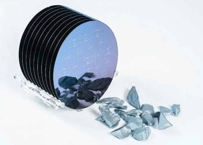
High-purity silicon is grown into single-crystal ingots and sliced into wafers before device fabrication. Sekisui describes the Czochralski crystal-growth method as a common route in which a seed crystal is gradually pulled from molten silicon to create a single-crystal ingot.
Silicon Carbide And Other Compound Semiconductors
Silicon carbide and other compound semiconductors are used when an application requires electrical, thermal, optical, voltage, or frequency performance that conventional silicon may not provide efficiently.
Important semiconductor materials include:
- Silicon carbide (SiC)
- Gallium nitride (GaN)
- Gallium arsenide (GaAs)
- Germanium (Ge)
- Indium phosphide (InP)
SiC and GaN are particularly important in power electronics, high-frequency electronics, electric vehicles, chargers, renewable energy, and industrial power systems.
Why Semiconductor Material Purity Matters
Semiconductor material purity matters because extremely small concentrations of unwanted contaminants can change electrical behavior or introduce defects during wafer fabrication.
Controlled doping is useful because dopant concentration and location are deliberately engineered. Uncontrolled contamination is different because it can alter threshold voltage, leakage, film adhesion, junction behavior, reliability, or yield.
Sekisui emphasizes that high purity and good crystallinity are essential during silicon preparation and crystal growth because even small unwanted impurities can contribute to downstream defects.
How Does The Semiconductor Manufacturing Industry Chain Work?
The semiconductor manufacturing industry chain moves from chip design and material production to wafer fabrication, packaging, testing, and final semiconductor devices. Different companies may specialize in one stage or integrate several stages within the same organization.
The physical manufacturing process is only one part of the broader semiconductor ecosystem. Chip designers, wafer suppliers, chemical manufacturers, equipment builders, foundries, packaging companies, test providers, and precision equipment suppliers all contribute to the final product.
Semiconductor Design
Semiconductor design determines the circuit architecture, transistor arrangement, interfaces, physical layout, and performance targets before wafer fabrication begins.
Design teams create the circuit information that eventually becomes mask patterns used during photolithography. A design error discovered after tape-out can be extremely expensive because new masks, fabrication cycles, and validation may be required.
Wafer And Raw Material Production
Wafer and raw material production supplies the high-purity substrates, photomasks, photoresists, process chemicals, gases, metals, and specialty materials required for fabrication.
Silicon preparation generally involves purification, crystal growth, slicing, polishing, cleaning, and inspection before a wafer is ready for device fabrication.
Wafer Fabrication
Wafer fabrication creates transistors and electrical structures on the wafer through repeated patterning, deposition, etching, doping, cleaning, planarization, and metallization operations.
Sekisui places foundry manufacturing in the middle of the semiconductor value chain, where circuit designs are physically converted into working structures on wafers.
Packaging And Testing
Packaging and testing protect individual dies, establish electrical connections, create heat-transfer paths, and verify whether the finished devices meet their performance requirements.
Packaging may use wire bonding, flip-chip interconnection, substrates, encapsulation, thermal materials, or advanced multi-die integration depending on the product.
Finished Semiconductor Devices
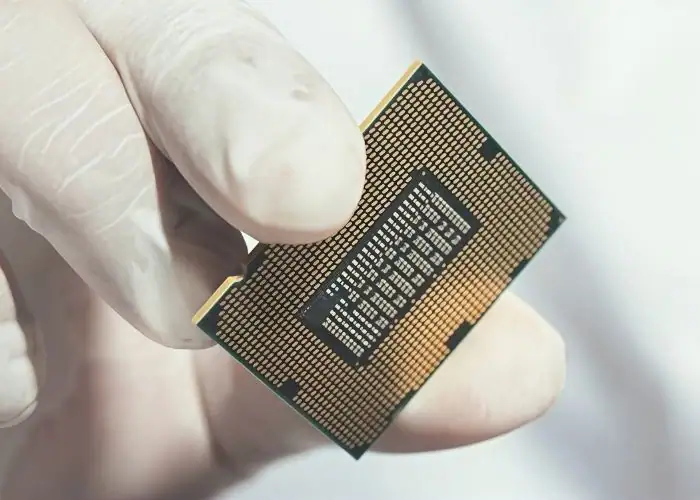
Finished semiconductor devices are tested and packaged chips ready to be integrated into electronic systems.
Examples include CPUs, GPUs, memory devices, microcontrollers, power MOSFETs, diodes, sensors, RF devices, and application-specific integrated circuits.
What Are Front-End And Back-End Semiconductor Manufacturing?
Front-end semiconductor manufacturing creates the electronic devices and circuits on a wafer, while back-end manufacturing separates, packages, connects, and tests individual dies after wafer fabrication.
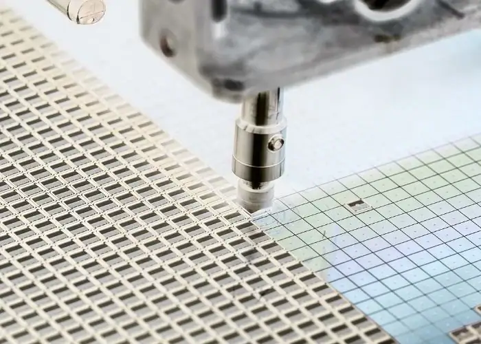
Bosch describes the main handoff as occurring after wafer-level electrical testing. Front-end work is primarily wafer processing, back-end work converts usable dies into packaged components.
| Factor | Front-End | Back-End |
| Main object | Wafer | Individual die/package |
| Main goal | Build electrical structures | Protect and connect chips |
| Lithography | Yes | Usually not conventional FEOL lithography |
| Etching/deposition | Extensive | Process-dependent |
| Dicing | No | Yes |
| Packaging | No | Yes |
| Final testing | Limited wafer test | Extensive final test |
Front-End Wafer Fabrication
Front-end wafer fabrication forms transistors, contacts, dielectric layers, and interconnect structures on the semiconductor substrate.
Typical front-end processes include oxidation, lithography, deposition, etching, ion implantation, thermal processing, cleaning, and CMP.
These operations may be repeated many times before the complete circuit is formed.
Back-End Assembly And Testing
Back-end semiconductor manufacturing separates dies from the wafer, attaches them to packages or substrates, creates electrical connections, protects them, and performs final testing.
Common operations include:
- Wafer thinning
- Wafer probing
- Dicing
- Die attach
- Wire bonding or flip-chip joining
- Encapsulation
- Package inspection
- Electrical testing
- Reliability testing
- Final packing
Key Differences Between Front-End And Back-End Processes
The key difference is that front-end processing creates the semiconductor device structures, while back-end processing turns those structures into physically usable packaged products.
Advanced packaging is making this division less simple than it once was because technologies such as chiplets, wafer-level packaging, 2.5D integration, and 3D stacking introduce increasingly sophisticated processing after conventional wafer fabrication.
Semiconductor Manufacturing Process Flow At A Glance
The semiconductor manufacturing process flow begins with high-purity material and wafer preparation, continues through repeated device-fabrication steps, and ends with wafer testing, dicing, packaging, and final electrical verification.
A practical semiconductor manufacturing process flow chart is:
| Stage | Main Process | Purpose |
| 1 | Silicon purification | Produce semiconductor-grade material |
| 2 | Crystal growth | Form single-crystal ingot |
| 3 | Wafer slicing and polishing | Create flat wafer substrate |
| 4 | Oxidation / deposition | Build functional thin films |
| 5 | Photolithography | Transfer circuit patterns |
| 6 | Etching | Remove selected material |
| 7 | Doping | Create controlled electrical regions |
| 8 | CMP | Restore planar surface |
| 9 | Metallization | Create electrical interconnects |
| 10 | Wafer testing | Identify functional dies |
| 11 | Dicing | Separate individual dies |
| 12 | Packaging | Protect and connect the die |
| 13 | Final testing | Verify performance and reliability |
The actual wafer fabrication process flow is far more repetitive than this table suggests. Lithography, deposition, etching, cleaning, doping, and planarization can be repeated across many layers before a finished circuit exists.
What Are The Main Steps In Semiconductor Manufacturing?
The main semiconductor manufacturing steps are material purification, crystal growth, wafer preparation, thin-film formation, photolithography, etching, doping, planarization, metallization, wafer test, dicing, packaging, and final testing.
The exact sequence varies with the device architecture and semiconductor manufacturing technology. Logic processors, memory, power semiconductors, MEMS, analog ICs, and compound semiconductor devices do not all use identical process flows.
Step 1: Silicon Purification And Crystal Growth
Silicon purification and crystal growth create the high-purity crystalline material from which silicon wafers are manufactured.
Silicon is purified, melted, and converted into a single-crystal ingot. The Czochralski method uses a seed crystal that is rotated and gradually withdrawn from molten silicon to create a controlled crystal structure.
Crystal quality is critical because defects introduced at this stage can remain through later processing and reduce device yield.
Step 2: Wafer Slicing And Polishing
Wafer slicing and polishing convert the cylindrical semiconductor ingot into thin, flat substrates with extremely smooth surfaces.
Precision sawing separates the ingot into wafers. Subsequent grinding, lapping, polishing, cleaning, and inspection produce the flat surface required for lithography and multilayer processing.
Sekisui notes that insufficient wafer smoothness can prevent later lithography and etching operations from maintaining the required accuracy.
Step 3: Oxidation And Thin Film Deposition
Oxidation and thin-film deposition create insulating, conductive, protective, or functional layers on the wafer.
Thermal oxidation can grow silicon dioxide directly on silicon. Other materials are deposited through processes such as:
- CVD — Chemical Vapor Deposition
- PVD — Physical Vapor Deposition
- ALD — Atomic Layer Deposition
These methods allow manufacturers to build extremely thin films of metals, oxides, nitrides, and other materials required for modern semiconductor structures.
Step 4: Photolithography And Pattern Transfer
Photolithography transfers the circuit pattern onto selected regions of the wafer so subsequent processing occurs only where required.
In a simplified photolithography process in IC fabrication, photoresist is applied to the wafer, a mask or reticle defines the desired pattern, light exposes the resist, and the resist is developed to leave patterned regions.
Lithography is repeated at many stages because each layer of the device requires different geometric patterns.
Step 5: Etching
Etching in IC fabrication selectively removes material from areas defined during lithography.
The two broad categories are:
| Etching Method | Principle | Main Characteristic |
| Wet etching | Chemical liquids remove material | Fast but can etch laterally |
| Dry etching | Plasma/reactive gases remove material | Better directional control |
| RIE | Reactive plasma + ion bombardment | High precision and anisotropy |
Modern semiconductor structures increasingly rely on controlled dry etching because narrow, high-aspect-ratio features demand precise vertical profiles. Renesas identifies reactive ion etching and plasma etching as important techniques for increasingly complex devices.
Step 6: Doping And Ion Implantation
Doping changes the electrical properties of selected semiconductor regions by introducing precisely controlled impurity atoms.
Boron is commonly associated with P-type silicon, while phosphorus and other donor dopants can form N-type regions. Ion implantation accelerates dopant ions toward the wafer so concentration and depth can be controlled.
This is one of the key answers to how are CPU transistors made: microscopic transistor regions are created by repeatedly combining patterned structures, doping, deposition, etching, dielectric formation, and interconnect fabrication.
Step 7: Chemical Mechanical Planarization
Chemical mechanical planarization, or CMP, flattens the wafer after layers and structures create surface-height variation.
CMP combines controlled chemical action with mechanical polishing. A flat surface is necessary because subsequent lithography steps require consistent focus and pattern placement.
Fuji Electric includes CMP after multiple patterning and deposition cycles to maintain wafer uniformity.
Step 8: Metallization And Interconnect Formation
Metallization creates conductive paths that electrically connect transistors and other circuit elements across the chip.
Modern chips require multiple levels of interconnects separated by dielectric layers. These networks carry signals, clock information, power, and ground throughout the circuit.
Sekisui compares metal interconnects to a road network that connects the numerous individual semiconductor structures into a complete functioning circuit.
Step 9: Wafer Testing And Die Sorting
Wafer testing identifies functional and defective dies before packaging resources are spent on them.
Electrical probes contact test structures or pads on individual dies. Depending on the product, dies may simply be classified as pass/fail or divided into performance bins.
Tensoft notes that semiconductor sort operations can produce multiple output grades from a single processed wafer, making yield and product genealogy important manufacturing variables.
Step 10: Dicing, Packaging, And Final Testing
Dicing, packaging, and final testing separate usable dies, protect them, provide external electrical connections, and confirm finished-device performance.
Wafer dicing can use precision saws or laser-based processes to separate individual dies. The dies may then be attached to substrates and connected through wire bonding, flip-chip, or other packaging technologies.
Final tests can verify electrical function, frequency, power consumption, thermal behavior, reliability, and other product-specific parameters.
How Does Photolithography Work In Semiconductor Manufacturing?
Photolithography works by coating a wafer with light-sensitive photoresist, exposing selected areas through a patterned mask or optical system, developing the resist, and using the resulting pattern to control later etching, implantation, or deposition operations.
Photoresist Coating
Photoresist coating applies a thin, controlled film of photosensitive material to the wafer.
Uniform thickness matters because variations can affect exposure and final pattern dimensions. After coating, thermal steps may be used to stabilize the film before exposure.
Mask Alignment And Exposure
Mask alignment and exposure position the desired circuit pattern over the correct wafer features and use controlled radiation to alter the photoresist.
Overlay accuracy becomes increasingly important as multiple patterned layers accumulate. Errors between layers can prevent transistors or interconnections from functioning correctly.
Pattern Development
Pattern development selectively removes soluble regions of exposed or unexposed photoresist depending on whether positive or negative resist chemistry is used.
The remaining resist acts as a temporary protective mask for the next manufacturing operation.
Pattern Transfer To The Wafer
Pattern transfer converts the resist geometry into physical or electrical structures on the wafer.
Depending on the process, the exposed areas may be etched, implanted, deposited, oxidized, or otherwise modified.
Renesas identifies advanced pattern-transfer technology, including EUV lithography and multi-patterning, as a key enabler of increasingly small and complex chip features.
How Do Deposition, Etching, And Doping Work Together?
Deposition, etching, and doping work together by adding material, selectively removing material, and changing electrical properties in precisely defined wafer regions. Repeating these three functions with lithography allows microscopic devices to be built layer by layer.
The processes are complementary rather than interchangeable:
| Process | What It Does | Result |
| Deposition | Adds a thin material layer | Films, dielectrics, conductors |
| Lithography | Defines pattern location | Process mask |
| Etching | Removes selected material | Physical geometry |
| Doping | Changes electrical behavior | P-type/N-type regions |
| CMP | Flattens surface | New process-ready plane |
Thin Film Deposition
Thin-film deposition adds controlled layers of material to the wafer using methods such as CVD, PVD, or ALD.
Different deposition technologies are selected according to thickness, conformality, material chemistry, temperature limits, and device architecture. ALD is particularly valuable where extremely controlled, conformal films are required.
Wet And Dry Etching
Wet and dry etching remove unwanted material after lithography defines the regions that must remain or be removed.
Wet etching can be economical and selective, while plasma-based dry etching can provide greater directional control for very small features.
The choice depends on material system, geometry, selectivity, critical dimension, and acceptable surface damage.
Diffusion And Ion Implantation
Diffusion and ion implantation introduce dopants that modify semiconductor conductivity.
Diffusion relies on high-temperature movement of atoms into the semiconductor, while ion implantation accelerates charged dopant particles toward the wafer.
Modern device fabrication typically requires tight control of dopant dose, depth, activation, and lateral distribution.
Repeating The Process To Build Multiple Layers
Repeated deposition, patterning, etching, doping, and planarization build the many active and interconnection layers of a semiconductor device.
Fuji Electric notes that advanced chips can contain dozens of layers, while Sekisui explains that major wafer processing steps may be repeated dozens or even more than one hundred times during fabrication.
What Is Metallization In Semiconductor Manufacturing?
Metallization in semiconductor manufacturing is the process of forming conductive metal structures that connect transistors and other device elements into functional electrical circuits.
Without metallization, individual transistor structures would exist but could not efficiently exchange signals, power, or data across the chip.
Metal Interconnect Formation
Metal interconnect formation creates conductive lines and vias on or within the wafer structure.
Modern interconnection fabrication typically involves combinations of deposition, patterning, etching, barrier layers, filling, and CMP.
Multiple interconnect levels may be stacked vertically to connect increasingly complex circuits.
Connecting Transistors And Circuit Layers
Metallization connects individual transistors into logic gates, memory cells, signal paths, power networks, and complete functional circuits.
The lowest interconnect layers typically handle very local connections, while upper layers can distribute signals and power across larger regions of the chip.
Why Interconnect Resistance Matters
Interconnect resistance matters because conductive paths consume energy and introduce delay as electrical signals travel through the chip.
As structures become smaller, resistance, capacitance, current density, electromigration, and heat can become increasingly important design limits.
Metallization is therefore both a manufacturing process and a major part of semiconductor electrical performance.
Why Are Semiconductor Packaging And Testing Important?
Semiconductor packaging and testing are important because the fabricated die must be mechanically protected, electrically connected, thermally managed, and verified before it can operate reliably in a real electronic product.
Sekisui identifies three central packaging roles: mechanical protection, thermal management, and electrical connection. Testing then determines whether the device satisfies required functional and quality criteria.
Wafer Testing And Electrical Wafer Sort
Electrical wafer sort tests dies before separation to identify which devices meet specification.
Probe equipment makes controlled electrical contact with wafer pads and can evaluate functionality or performance parameters.
Early detection reduces the cost of packaging defective dies.
Semiconductor Dicing
Semiconductor dicing separates the processed wafer into individual dies.
Precision saws and laser technologies are commonly used. Kerf width, edge chipping, contamination, stress, and die strength must be controlled because dicing occurs after substantial value has already been added to the wafer.
Chip Packaging And Assembly
Chip packaging and assembly attach the die to a package or substrate and create electrical connections to the outside system.
Common technologies include:
- Wire bonding
- Flip-chip
- Ball grid arrays
- Wafer-level packaging
- Fan-out packaging
- 5D integration
- 3D stacking
- System-in-Package
Renesas highlights 3D packaging, fan-out packaging, and SiP as approaches for increasing integration density and improving system functionality.
Semiconductor Packaging Materials
Semiconductor packaging materials protect the die while supporting electrical connection and thermal management.
Typical material categories include substrates, encapsulants, underfills, adhesives, die-attach materials, solder, copper interconnects, thermal interface materials, and insulating films.
The correct material system depends on operating temperature, package size, coefficient of thermal expansion, electrical requirements, moisture sensitivity, and reliability target.
Final Electrical And Reliability Testing
Final testing verifies that packaged devices meet electrical and reliability specifications before shipment.
Testing can include:
- Functional test
- Parametric test
- Power consumption
- Frequency
- Leakage current
- Temperature cycling
- Burn-in
- Mechanical reliability
- Package inspection
Only devices that satisfy the required acceptance criteria move into finished inventory.
What Equipment Is Used In Semiconductor Manufacturing?
Semiconductor manufacturing uses lithography systems, deposition chambers, etchers, ion implanters, CMP tools, cleaning systems, metrology equipment, wafer handlers, testers, packaging machines, vacuum systems, and extensive automated support equipment.
A modern fab is therefore not one production machine. It is an interconnected manufacturing environment involving many highly specialized equipment families.
Lithography Equipment
Lithography equipment transfers highly controlled geometric patterns onto wafer photoresist.
Systems can include coat/develop tracks, scanners, alignment systems, masks or reticles, optical systems, stages, environmental controls, and measurement equipment.
Deposition Equipment
Deposition equipment forms thin films through processes including CVD, PVD, ALD, epitaxy, and related technologies.
Different chambers are optimized for specific materials, film thicknesses, temperatures, gas chemistries, and wafer sizes.
Etching Equipment
Etching equipment selectively removes semiconductor, dielectric, or metal layers.
Wet benches use liquid chemistry, while dry etch tools use reactive gases and plasma to achieve more directional feature profiles.
Ion Implantation And Doping Equipment
Ion implantation equipment introduces controlled dopant species into predefined wafer regions.
The equipment controls parameters such as ion species, energy, dose, beam distribution, and wafer position.
CMP And Wafer Polishing Equipment
CMP equipment combines chemical slurry and mechanical action to create a highly planar wafer surface.
Planarity is critical because subsequent photolithography processes must maintain focus across increasingly complex multilayer structures.
Metrology And Inspection Equipment
Metrology and inspection equipment measure dimensions, film thickness, defects, overlay, surface condition, electrical characteristics, and other critical manufacturing parameters.
Data from these tools supports process control, root-cause analysis, yield improvement, and equipment adjustment.
Wafer Testing And Packaging Equipment
Wafer testing and packaging equipment handles probing, die sorting, dicing, die attach, bonding, encapsulation, inspection, and final electrical test.
Back-end automation must maintain both throughput and traceability because one wafer can generate many individual dies with different performance grades.
How Are Semiconductor Equipment Components Manufactured?
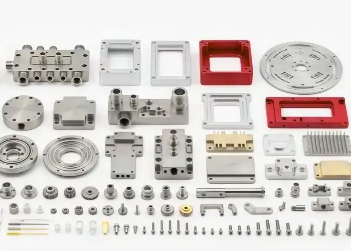
Semiconductor equipment components are manufactured through CNC machining, sheet metal fabrication, precision grinding, EDM, welding, additive manufacturing, surface finishing, and precision cleaning according to each component’s geometry, material, cleanliness, vacuum, thermal, and accuracy requirements.
These processes manufacture the mechanical equipment around semiconductor wafer processing, they do not replace wafer-level photolithography, etching, implantation, or deposition.
CNC Machining
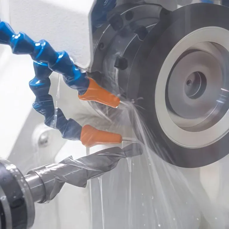
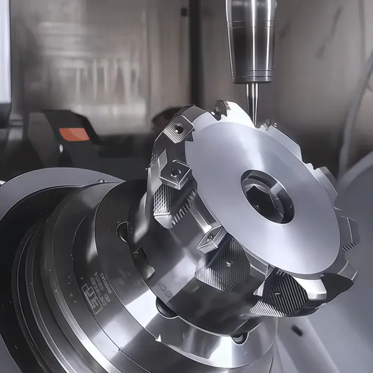
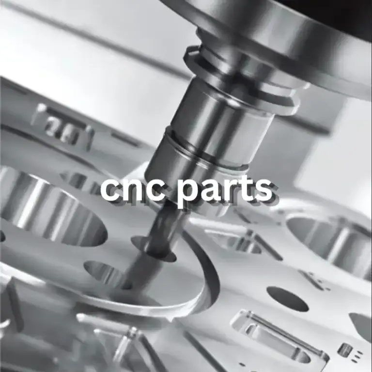
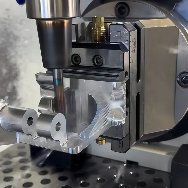
CNC machining is one of the primary methods for producing precision semiconductor equipment components such as chambers, fixtures, bases, cooling plates, robotic interfaces, housings, sensor mounts, manifolds, and positioning components.
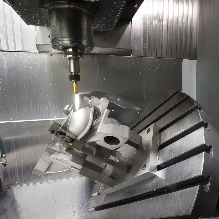
CNC milling, turning, drilling, boring, tapping, and 5-axis machining may be combined according to geometry. Common materials include aluminum, stainless steel, copper, PEEK, PTFE, and other engineering materials.
For semiconductor equipment, drawings may need to control not only dimensional tolerance but also:
- Flatness
- Parallelism
- Surface roughness
- Burr condition
- Sealing surfaces
- Particle generation
- Cleaning requirements
- Surface treatment
- Vacuum compatibility
Sheet Metal Fabrication
Sheet metal fabrication is used for machine enclosures, brackets, panels, guards, cabinets, trays, covers, and large thin-wall equipment structures.
Laser cutting, punching, bending, forming, fastening, and hardware insertion can produce these components with much lower material waste than machining a large enclosure from solid billet.
Precision Grinding
Precision grinding is used for reference surfaces, machine bases, stages, precision plates, hardened components, and parts requiring tight flatness or parallelism.
A common manufacturing strategy is to CNC machine the majority of the geometry and leave controlled stock on critical surfaces for final grinding.
EDM
EDM is used for electrically conductive components that contain narrow slots, deep cavities, difficult internal geometry, hardened materials, or features inaccessible to conventional cutting tools.
Wire EDM is particularly suitable for through profiles and precision slots, while sinker EDM can produce detailed cavities.
Welding And Fabrication
Welding and fabrication are used for larger machine structures, stainless steel assemblies, supports, frames, and fluid or vacuum-related hardware.
Distortion control is important because welding heat can affect alignment, flatness, or sealing interfaces. Critical welded assemblies may therefore require post-weld machining and inspection.
Additive Manufacturing
Additive manufacturing is used for prototypes, lightweight structures, complex internal passages, development tooling, and low-volume semiconductor equipment parts.
It can produce geometries difficult to machine conventionally, but precision interfaces commonly require secondary CNC machining or grinding.
Surface Finishing And Precision Cleaning
Surface finishing and precision cleaning prepare equipment components for corrosion resistance, wear resistance, vacuum service, contamination control, or cosmetic requirements.
Possible processes include anodizing, electroless nickel plating, passivation, polishing, electropolishing, bead blasting, ultrasonic cleaning, DI-water cleaning, and controlled packaging.
For sensitive semiconductor environments, residual oils, particles, burrs, polishing compounds, and cleaning chemistry may matter as much as the nominal part tolerance.
What Is A Semiconductor Fab?
A semiconductor fab is a specialized production facility containing cleanrooms, wafer-processing equipment, utilities, automation, chemical systems, gas delivery, vacuum infrastructure, metrology, and environmental controls needed to manufacture semiconductor devices.
Fabs are often described by wafer size, process technology, device family, and production capability. Bosch notes that common wafer diameters include 200mm and 300mm and that facilities may specialize in different technology nodes or device categories.
Cleanroom And Contamination Control
Cleanrooms control airborne particles and environmental conditions that could damage microscopic semiconductor structures.
Contamination control can include:
- HEPA or ULPA filtration
- Controlled airflow
- Temperature control
- Humidity control
- Gowning protocols
- Chemical management
- Material restrictions
- Particle monitoring
The acceptable contamination level depends on the process and technology.
Process Equipment And Automation
Process equipment and automation move wafers through carefully defined fabrication recipes while minimizing handling and contamination.
Automated material-handling systems, wafer robots, load ports, process chambers, sensors, MES platforms, and inspection systems coordinate production across many different operations.
Water, Gas, Chemical, And Vacuum Systems
Water, gas, chemical, and vacuum systems provide the controlled process environment semiconductor equipment needs.
Fabs rely on ultra-pure water, high-purity gases, specialty chemicals, vacuum pumps, exhaust treatment, temperature control, and sophisticated safety systems.
These utility systems can be as important to process stability as the wafer-processing tool itself.
What Makes A Semiconductor Fab State Of The Art?
A state-of-the-art semiconductor fab combines advanced process capability, high-quality equipment, sophisticated automation, stable yield, contamination control, and the ability to manufacture the intended device technology economically.
Bosch notes that “state of the art” is application-dependent rather than defined by one universal process node. Advanced logic fabs may focus on very small nodes, while power-semiconductor, MEMS, analog, or compound-semiconductor fabs have different technical priorities.
Why Is Semiconductor Manufacturing So Complex?
Semiconductor manufacturing is complex because billions of microscopic structures must be created across repeated process layers while maintaining extremely tight dimensional, electrical, chemical, cleanliness, and yield requirements.
A process error near the end of production can destroy value accumulated across many prior steps.
The main reasons include:
- Nanometer-scale critical dimensions
- Hundreds of manufacturing operations
- Repeated lithography and pattern-transfer cycles
- Tight overlay requirements
- Extreme contamination sensitivity
- Complex material interactions
- Expensive equipment
- Long cycle times
- Difficult defect detection
- Yield dependence
- Extensive process traceability
Bosch cites 200–1,000+ individual process steps in semiconductor manufacturing, while Renesas notes that wafer fabrication may require hundreds of operations and can extend to roughly 16–18 weeks for some processes.
What Are The Main Bottlenecks In Semiconductor Manufacturing?
The main semiconductor manufacturing bottlenecks are lithography availability, equipment capacity, yield loss, wafer defects, process complexity, advanced packaging capacity, long qualification cycles, material supply, and cleanroom capacity.
A bottleneck does not necessarily occur at the process with the longest nominal cycle time. A specialized tool with high utilization can constrain the entire manufacturing line even when other equipment has spare capacity.
Lithography And Pattern Transfer Limits
Lithography can become a bottleneck because advanced patterning equipment is technically complex, costly, and required repeatedly during wafer fabrication.
Smaller features also demand tighter overlay, mask accuracy, resist behavior, and process control.
Equipment Capacity And Production Throughput
Equipment capacity limits output when a required tool family cannot process wafers fast enough to meet demand.
Bosch specifically identifies lithography availability, cleanroom capacity, specialized equipment, and yield optimization as common manufacturing constraints.
Yield Loss And Wafer Defects
Yield loss reduces the number of usable dies produced from each wafer.
Particles, process variation, crystal defects, lithography errors, etch defects, contamination, electrical faults, and packaging damage can all reduce yield.
Because semiconductor manufacturing adds value over many weeks, late-stage yield loss can be particularly expensive.
Advanced Packaging Capacity
Advanced packaging can become a production constraint as more systems rely on chiplets, 2.5D structures, 3D integration, high-density interconnects, and high-bandwidth memory.
Packaging is increasingly a performance technology rather than simply a protective final step.
Materials And Supply Chain Constraints
Material and supply constraints can affect production because semiconductor fabrication depends on specialized wafers, gases, photoresists, masks, chemicals, substrates, equipment components, and packaging materials.
Many of these inputs require long qualification periods, so substitutes cannot always be introduced quickly.
What Are The Current Trends And Challenges In Semiconductor Manufacturing?
Current semiconductor manufacturing trends include smaller and more complex device structures, advanced packaging, wide-bandgap materials, higher automation, stronger yield analytics, growing AI-driven demand, and continued expansion of fabrication capacity. The major challenges remain cost, complexity, equipment availability, energy use, supply risk, and process yield.
Renesas identifies pattern transfer, doping, deposition, etching, and packaging as process areas undergoing continued technical development.
Smaller Process Nodes And Higher Device Density
Smaller process nodes increase the number and density of electronic functions that can be integrated into advanced chips.
However, continued scaling also increases lithography complexity, interconnect challenges, thermal density, process control requirements, and capital cost.
Advanced Semiconductor Packaging
Advanced semiconductor packaging is increasingly used to improve system performance without relying exclusively on monolithic transistor scaling.
3D packaging, fan-out, SiP, chiplets, and high-density interconnect technologies can combine multiple dies or functions within one integrated package.
Silicon Carbide And Wide-Bandgap Semiconductors
Silicon carbide and other wide-bandgap semiconductor technologies are expanding in applications where high voltage, switching efficiency, temperature, and power density matter.
EV inverters, charging equipment, renewable-energy systems, industrial drives, and power supplies are important application areas.
Increasing Equipment And Fab Costs
Fab and equipment costs continue to rise because advanced manufacturing requires increasingly specialized tools, facilities, utilities, automation, metrology, and process integration.
Fuji Electric notes that semiconductor fabs require investment measured in billions of dollars and that yield directly affects manufacturing economics.
Yield Improvement And Process Control
Yield improvement remains central because even a technically successful fabrication process can be economically weak if too many dies fail.
Advanced metrology, automated inspection, statistical process control, equipment monitoring, defect classification, and manufacturing data analytics are therefore integral parts of semiconductor manufacturing technology.
Expanding Global Manufacturing Capacity
Global semiconductor manufacturing capacity is expanding as chip demand grows and governments seek greater supply-chain resilience.
SIA reported that worldwide semiconductor sales reached $795.6billion in 2025 and projected the market to exceed $1.5trillion in 2026, driven strongly by AI and advanced computing demand.
FAQs
What Is Dying In Semiconductor Manufacturing?
“Dying” is not a standard semiconductor manufacturing term, the intended term is usually dicing, which separates a completed wafer into individual dies or chips. After wafer-level testing, precision diamond saws or laser processes cut along designated streets between dies. Dicing quality affects edge chipping, particle generation, die strength, and downstream packaging yield. Fuji Electric identifies wafer dicing as the stage where the processed wafer is separated into individual semiconductor chips before packaging.
What Is Metallization In Semiconductor Manufacturing?
Metallization in semiconductor manufacturing creates conductive interconnects that electrically connect transistors, contacts, power networks, and circuit layers. Conductive films are deposited and patterned to form lines and vertical connections, often across multiple interconnect levels. Resistance, capacitance, electromigration, film thickness, adhesion, and interface quality directly affect chip speed and reliability. Sekisui describes metal wiring as the network that connects large numbers of transistors so signals can travel through the finished circuit.
Which Country Is The Largest Producer Of Semiconductors?
By installed wafer fabrication capacity, China was the largest manufacturing location in SIA’s 2025 industry report, accounting for about 27% of global capacity in 2024, followed by Taiwan at 18%, South Korea at 16%, and Japan at 15%. However, leadership changes by metric: Taiwan remains especially strong in advanced foundry manufacturing, while South Korea is dominant in memory and the U.S. leads semiconductor-company sales and design. The metric should therefore always be specified.
Conclusion
Semiconductor manufacturing transforms high-purity semiconductor material into functional electronic devices through an exceptionally controlled sequence of crystal growth, wafer preparation, photolithography, deposition, etching, doping, CMP, metallization, testing, dicing, packaging, and final inspection. Understanding the complete semiconductor process requires viewing front-end wafer fabrication and back-end packaging together while also considering equipment precision, contamination control, yield, materials, automation, and increasingly complex advanced packaging technologies.
At TiRapid, we provide precision CNC machining and custom manufacturing services for components used in semiconductor equipment, automation, electronics, and other precision systems. Our capabilities include CNC milling, CNC turning, 5-axis CNC machining, sheet metal fabrication, EDM, precision finishing, surface treatment, and dimensional inspection for aluminum, stainless steel, copper, engineering plastics, and other custom components used in prototype and low-volume equipment manufacturing.