Semiconductor equipment depends on far more than electronics and process technology. Behind every wafer-handling system, test station, inspection tool, and process chamber is a network of precision-machined parts, structural components, fixtures, enclosures, and motion hardware that must work together with exceptional consistency.
This guide explains how semiconductor equipment hardware is manufactured, how precision and cleanliness affect engineering decisions, and where CNC machining, sheet metal fabrication, molding, and standard components fit into the system. It also covers DFM, materials, sourcing decisions, cost, and supplier coordination.
What Is Semiconductor Equipment Manufacturing?
Semiconductor equipment manufacturing is the production of mechanical hardware used to fabricate, handle, inspect, test, clean, and assemble semiconductor devices. Unlike chip fabrication itself, the focus here is on the machines, fixtures, structures, and precision components that make semiconductor production possible.
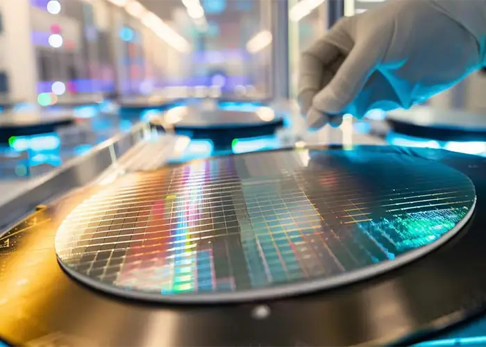
Precision Hardware Behind Semiconductor Production
Semiconductor production moves through front-end wafer processing and back-end assembly and testing, and each stage relies on dedicated equipment. Mechanical hardware may position wafers, control gas or fluid delivery, support sensors, hold test devices, or provide stable interfaces between motion and process systems.
The manufacturing challenge is therefore broader than achieving a single tight dimension. Components must maintain geometry, alignment, cleanliness, and repeatability after assembly and under actual operating conditions.
Common Equipment, Components, and Assemblies
Typical hardware includes brackets, precision plates, IC test socket components, wafer-holding fixtures, valve bodies, pump components, equipment housings, and chamber-related parts. Semiconductor equipment also integrates motion systems, bearings, guides, connectors, seals, and structural frames.
Some parts require precision machining, while others are better produced by sheet metal fabrication, molding, or purchased as standardized components. Selecting the right process for each part is central to both system performance and manufacturing cost.
System-Level Manufacturing Decisions in Semiconductor Equipment
Semiconductor hardware operates as an integrated system. Precision, thermal behavior, cleanliness, motion, structural rigidity, and assembly repeatability can all affect equipment performance, so manufacturing decisions should not be made from individual drawings alone.
Precision and Tolerance Requirements Across the System
Not every part requires the same tolerance. Wafer-handling interfaces, alignment components, test fixtures, and precision locating surfaces may require closely controlled flatness, parallelism, position, and repeatability. Structural covers and non-critical brackets often do not.
Applying unnecessarily tight tolerances throughout a machine increases machining and inspection effort without necessarily improving equipment performance. A better approach is to identify the dimensions and datums that directly control alignment, motion, sealing, or assembly.
Thermal Stability and Mechanical Integration
Temperature changes can alter dimensions and alignment through thermal expansion. This matters particularly when precision stages, optical assemblies, wafer-handling hardware, and long structural members interact within the same machine.
Material selection, component geometry, stiffness, joint design, and tolerance strategy should therefore be evaluated together. A part that meets its drawing at inspection can still create problems if the complete assembly responds poorly to operating temperature changes.
Repeatability, Alignment, and Motion Control
Semiconductor equipment frequently performs the same motion or positioning operation thousands of times. Reliable performance depends on locating features, mating surfaces, bearings, guides, and machined interfaces returning to predictable positions.
Repeatability is therefore influenced by more than machine accuracy. Datum selection, fastener location, dowel features, contact surfaces, component stiffness, and assembly sequence all affect how consistently a system can be built and serviced.
Key Manufacturing Processes for Semiconductor Equipment
Modern semiconductor equipment combines several manufacturing methods. Precision machining is used where geometry and alignment are critical, while fabrication and molding can provide efficient solutions for larger structural or non-metallic components.
Precision CNC Machining for Semiconductor Components
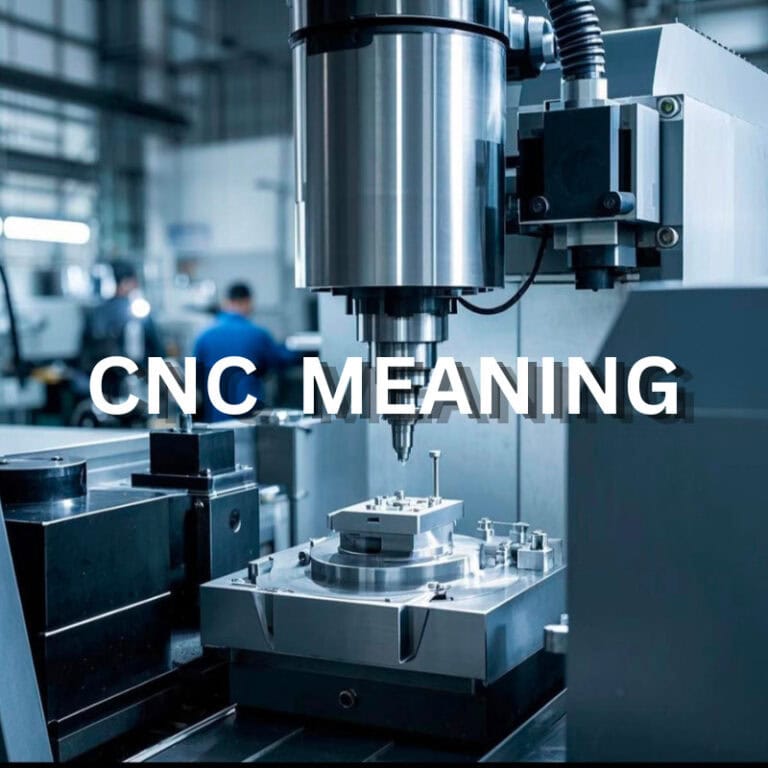
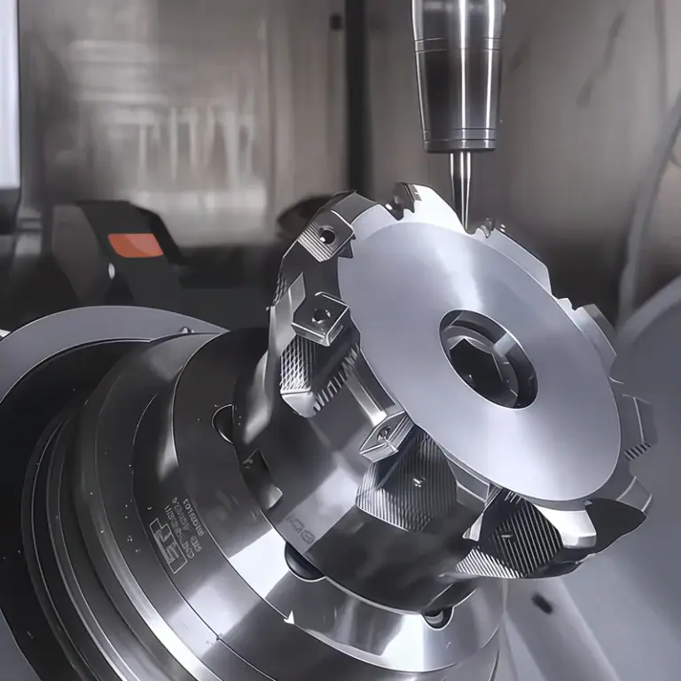
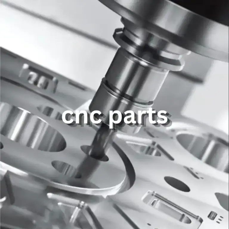
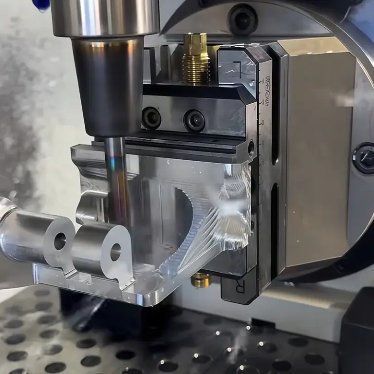
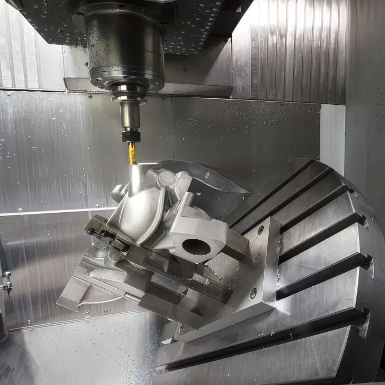
CNC machining is widely used for alignment-critical components, fixtures, precision plates, housings, brackets, manifolds, valve components, and other hardware with demanding geometric requirements. Common considerations include flatness, parallelism, hole position, sealing surfaces, surface finish, and repeatable datum relationships.
Aluminum alloys such as 6061 and 7075 are common where low weight and machinability are important. Stainless steels such as 304 and 316L are considered where corrosion resistance or process compatibility matters, while engineering plastics such as PEEK and PEI can provide electrical insulation or reduced weight.
Test Fixtures and Burn-In Hardware
Semiconductor test fixtures must maintain repeatable mechanical and electrical contact between devices and test systems. Alignment plates, socket bodies, support structures, and interfaces around pogo-pin arrays can require closely controlled positions because small shifts may affect electrical contact.
Burn-in hardware introduces additional thermal requirements. Fixture materials and assembly structures must remain stable during repeated exposure to elevated temperature and electrical loading, making tolerance stack-up, insulation, wear, and dimensional stability important design factors.
Sheet Metal Fabrication for Frames and Enclosures
Sheet metal is well suited to equipment covers, electrical enclosures, panels, racks, brackets, shields, and other structural elements that do not require extensive machining.
Bend accuracy, joining methods, frame stiffness, and interface location still matter when fabricated structures support precision assemblies. Enclosures may also require electromagnetic shielding, controlled openings, and surfaces that are easy to clean.
Injection Molding for Housings and Insulating Components
Injection molding can be suitable for repeat-production housings, cable-management features, covers, and electrical insulation components. Complex features can often be integrated into one molded part, reducing secondary assembly.
For cleanroom or vacuum applications, resin selection requires additional care. Additives, lubricants, release agents, and the polymer itself should be evaluated for particle generation, chemical compatibility, and outgassing rather than selecting a material only for mechanical performance.
Design for Manufacturability in Semiconductor Equipment
DFM for semiconductor equipment should address the complete assembly rather than simply making each component easier to manufacture. Interface control, assembly repeatability, maintenance, and production consistency are often more important than optimizing one isolated feature.
Managing Tolerance Stack-Up
A series of individually acceptable components can still create an unacceptable assembly when dimensional variation accumulates.
Critical mechanical chains should therefore be identified early. Designers can control stack-up by establishing clear datums, limiting unnecessary intermediate interfaces, assigning tighter tolerances only where function requires them, and allowing adjustment where practical.
Designing Reliable Alignment Features
Dowel pins, locating shoulders, precision bores, keyed interfaces, and controlled mating surfaces can make assembly more repeatable.
These features are particularly valuable when modules must be removed and reinstalled during maintenance. The goal is to let functional geometry establish position rather than relying solely on fastener clearance or manual adjustment.
Improving Modularity and Assembly Efficiency
Dividing equipment into functional modules can simplify manufacturing, inspection, assembly, and maintenance. Modules can be qualified independently before integration, making dimensional or functional problems easier to isolate.
Modularity also allows individual subsystems to evolve without requiring the entire machine architecture to be redesigned.
Designing for Service and Maintenance Access
Semiconductor production equipment must eventually be inspected, cleaned, adjusted, or repaired. Components that are difficult to reach can increase downtime even when the original manufacturing design is technically sound.
Fasteners, removable panels, cable routing, locating features, and replacement modules should therefore be considered during mechanical design rather than after assembly is complete.
Materials and Cleanroom Considerations
Material selection in semiconductor equipment is influenced by mechanical properties and environmental compatibility. Cleanliness, chemical exposure, vacuum conditions, corrosion, particle generation, and surface behavior can be as important as strength and machinability.
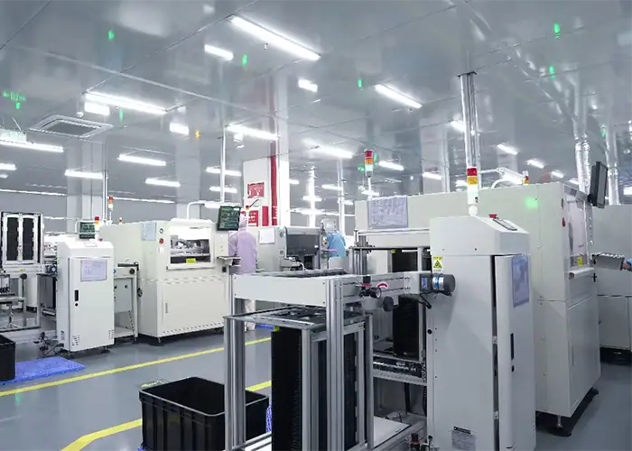
Materials for Precision and Structural Components
Aluminum is attractive for many precision and structural components because it combines low density, good machinability, and useful stiffness. Stainless steel offers greater corrosion resistance and can be appropriate for hardware exposed to demanding environments.
Engineering plastics can provide insulation, chemical resistance, or reduced mass, but creep, thermal expansion, moisture behavior, and dimensional stability must be considered before using them for precision interfaces.
Surface Finishes for Semiconductor Equipment Parts
Surface treatment should match the material and operating environment. Anodizing may improve aluminum surface durability, while passivation can improve the corrosion behavior of suitable stainless-steel components.
Finish selection should also consider cleaning requirements, sealing surfaces, electrical contact, vacuum performance, and chemical exposure. A coating that works well on general industrial equipment is not automatically appropriate for semiconductor process hardware.
Particle Control and Low-Outgassing Requirements
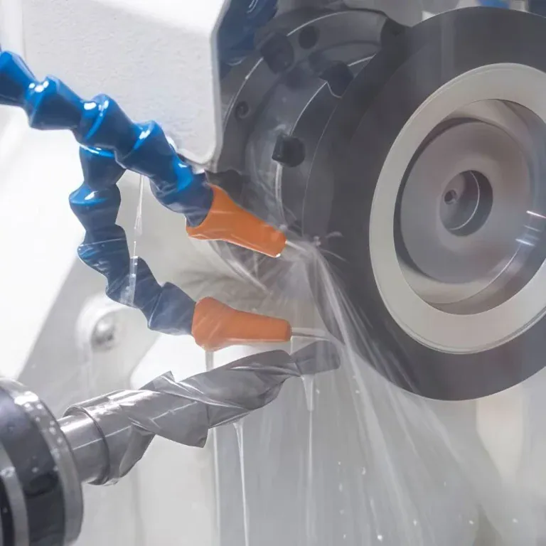
Equipment installed in controlled environments should avoid generating or retaining unnecessary contamination. Smooth, cleanable surfaces, appropriate materials, controlled cleaning, and suitable packaging help reduce particles, machining residue, oils, and other contaminants reaching sensitive areas.
Low-outgassing behavior becomes particularly important near wafers, optics, sensitive process zones, and vacuum environments. Material selection should therefore include environmental compatibility, not just strength or cost.
Vacuum and Chemical Compatibility
Vacuum components place additional demands on materials, joints, lubricants, seals, and surface condition. Semiconductor equipment can also encounter process gases and aggressive cleaning chemicals.
Chemical resistance needs to be evaluated against the actual substances and concentrations involved. Even commonly used materials such as aluminum may require protection or replacement when exposed to certain aggressive chemicals.
Using Standard and Custom Components in Semiconductor Systems
A semiconductor machine does not need every component to be custom manufactured. Combining proven standard hardware with purpose-built precision components can reduce development time while preserving performance where customization matters most.
Where Standard Components Make Sense
Bearings, linear guides, fasteners, connectors, sensors, and other established hardware are often better sourced as standard products when their specifications meet system requirements.
Using proven components can simplify replacement, shorten sourcing time, and reduce unnecessary engineering effort.
Where Custom Components Add More Value
Custom manufacturing becomes more valuable when the component controls a unique interface or directly influences equipment performance.
Wafer-handling components, test fixtures, precision mounting plates, manifolds, alignment hardware, and application-specific housings often need geometry that cannot be obtained from a standard catalog.
Combining Standard and Custom Hardware in One System
A practical machine frequently combines both. A precision linear guide may be purchased as a standard component while its mounting base, interface bracket, and alignment features are custom machined.
This allows engineers to use commercially proven motion hardware while tailoring the surrounding mechanical structure to the specific equipment.
Choosing Custom vs. Off-the-Shelf Components
The choice between custom and standard hardware should be based on function rather than preference. Precision, integration, production demand, replacement needs, and long-term availability all influence the decision.
Precision and Functional Requirements
Custom parts are appropriate when geometry, alignment, material, surface condition, or mating relationships are unique to the machine.
Standard components are preferable when an established product can meet the same function without compromising the surrounding assembly.
Production Volume and Design Flexibility
Custom machining provides substantial flexibility during prototypes and evolving equipment designs because geometry can be revised without dedicated production tooling.
As volume increases and a design becomes stable, molded or standardized solutions may become more economical for suitable components.
Cost, Availability, and Replacement Considerations
Initial part cost is only one factor. Availability, lead time, service life, replacement risk, and the cost of redesigning surrounding hardware should also be considered.
A low-cost proprietary component with uncertain future availability may create more long-term risk than a standardized alternative.
Cost and Lead Time Considerations in Semiconductor Equipment Manufacturing
Cost is driven by the complete manufacturing requirement rather than by process name alone. Geometry, material, tolerance, surface treatment, inspection, cleanliness, quantity, and assembly all influence the final result.
How Manufacturing Processes Affect Cost
CNC machining avoids dedicated molds and provides high geometric flexibility, making it useful for prototypes, low-volume production, and precision hardware. Sheet metal is often efficient for larger structures and enclosures, while molding can reduce unit cost for stable, higher-volume plastic components after tooling investment.
The most economical process is therefore the one that matches both the design and production quantity.
How Tolerances, Materials, and Finishes Affect Lead Time
Tighter tolerances can require additional machining passes, more stable setups, and more extensive inspection. Difficult materials may reduce cutting speed or increase tool wear.
Special coatings, cleaning, controlled packaging, and documentation can add further operations, so these requirements should be defined early rather than added after manufacturing begins.
Prototype, Low-Volume, and Production Requirements
Prototype equipment benefits from processes that allow rapid design changes. As the machine matures, the manufacturing strategy can shift toward repeatability, standardized tooling, efficient fixturing, and controlled production workflows.
Production planning should therefore reflect the current design stage rather than assuming the prototype method must remain unchanged at higher volume.
How to Choose the Right Manufacturing Approach
A good manufacturing strategy starts by identifying which requirements actually drive the part. Precision, cleanliness, quantity, geometry, material, and system integration should guide process selection.
Match the Process to Part Geometry and Precision
Complex precision interfaces, accurate holes, sealing surfaces, and controlled datum relationships often favor CNC machining. Large covers and structural panels may favor fabrication, while repeat plastic components may justify molding.
Selecting the process before understanding the geometry can create unnecessary restrictions later.
Consider Cleanroom and Material Requirements
Materials and finishes should be evaluated against the actual operating environment, including particles, chemicals, vacuum exposure, electrical behavior, and cleaning procedures.
This is especially important because manufacturing suitability does not automatically mean cleanroom or process compatibility.
Balance Production Volume, Cost, and Lead Time
Prototype quantities favor flexibility, while stable production volumes can justify more dedicated tooling and process optimization.
The lowest unit price is not always the lowest project cost if it requires expensive tooling, long qualification cycles, or reduced flexibility during design changes.
Plan for Assembly and System Integration
Individual parts should be evaluated in the context of their mating components. Datums, interfaces, fasteners, alignment features, and tolerance chains need to function together after manufacturing.
This system-level view reduces the risk of receiving individually compliant parts that still fail to assemble correctly.
Managing Sourcing and Integration Risk
Semiconductor equipment often combines parts from several processes and suppliers. The more interfaces involved, the more important drawing control, inspection strategy, communication, and ownership become.
Reducing Tolerance and Interface Mismatches
Two suppliers can manufacture parts within their respective drawing tolerances and still create an assembly problem if interface requirements were not defined correctly.
Shared datums, mating dimensions, inspection methods, and revision control should therefore be clear before production begins.
Coordinating Parts Made by Different Processes
Machined parts, fabricated structures, molded components, and purchased hardware behave differently in production.
Their tolerances, surface conditions, tooling constraints, and lead times should be coordinated at the assembly level rather than treating each sourcing package independently.
Maintaining Quality Across Multiple Suppliers
Supplier variation can affect dimensional consistency, documentation, finishing, cleaning, and packaging.
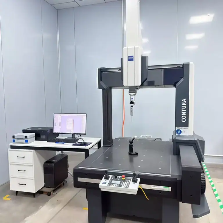
Clear specifications and consistent inspection criteria make it easier to identify problems early and prevent quality differences from appearing only during final assembly.
Why a Coordinated Manufacturing Partner Matters
A capable manufacturing partner should do more than reproduce CAD geometry. For complex semiconductor hardware, manufacturing feedback should help connect part design with machining feasibility, inspection, assembly, and production consistency.
Unified DFM and Engineering Communication
Centralized engineering feedback can identify difficult tolerances, inaccessible features, unstable setups, or interface risks before production.
This reduces repeated communication between design teams and separate manufacturing sources.
Coordinated Production and Quality Control
When critical components share mating surfaces or tolerance relationships, coordinated manufacturing and inspection can reduce variation between independently produced parts.
The objective is not simply tighter tolerances, but better control of the dimensions that determine system performance.
Simplifying Supply Chain and Project Management
Reducing unnecessary supplier fragmentation can simplify revision management, scheduling, quality communication, and accountability.
For precision-machined semiconductor hardware in particular, working with a supplier that understands complex geometry, material behavior, finishing, and dimensional inspection can make the transition from prototype to repeat production more predictable.
FAQs
What Is Semiconductor Manufacturing?
Semiconductor manufacturing is the process of producing electronic devices and integrated circuits on silicon wafers. It includes wafer preparation, deposition, lithography, etching, doping, cleaning, packaging, and testing. The process depends on highly controlled equipment, clean environments, and precision hardware.
How Are Semiconductors Made?
Semiconductors are made by building microscopic circuit structures layer by layer on a silicon wafer. Manufacturers use processes such as deposition, photolithography, etching, ion implantation, and cleaning before the wafer is tested, diced, packaged, and inspected.
Where Are Semiconductors Used?
Semiconductors are used in computers, smartphones, vehicles, industrial equipment, medical devices, communication systems, automation, aerospace systems, and consumer electronics. They support functions such as computing, sensing, power control, data storage, and signal processing.
Conclusion
Reliable semiconductor equipment manufacturing depends on controlling the relationships between parts, not simply producing each component to a drawing. Precision, thermal stability, material behavior, cleanliness, DFM, inspection, and sourcing strategy all influence the finished system. The strongest manufacturing approach applies tight requirements where they affect function while using practical processes and standard hardware wherever additional precision would add cost without improving performance.
At TiRapid, we provide precision CNC machining and manufacturing services for complex semiconductor equipment components in metals and engineering plastics. Our capabilities support prototype and low-volume parts, complex geometries, precision interfaces, material evaluation, surface finishing coordination, and dimensional inspection for demanding equipment hardware.