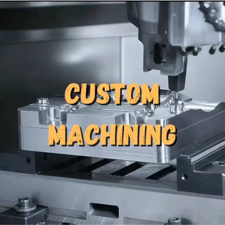
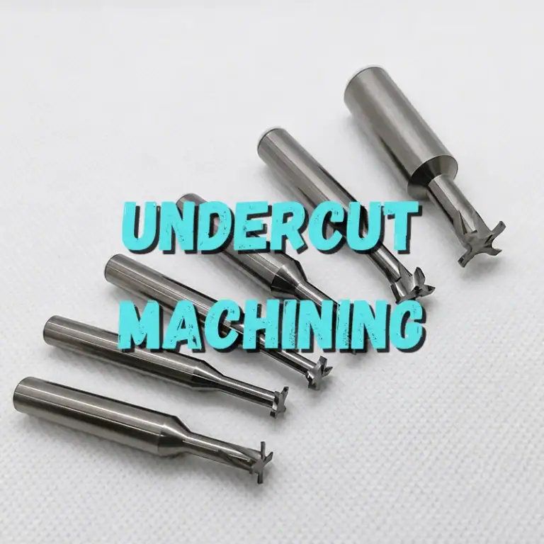
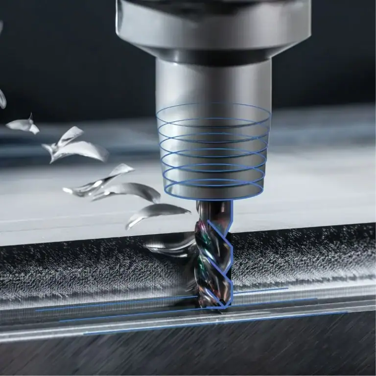
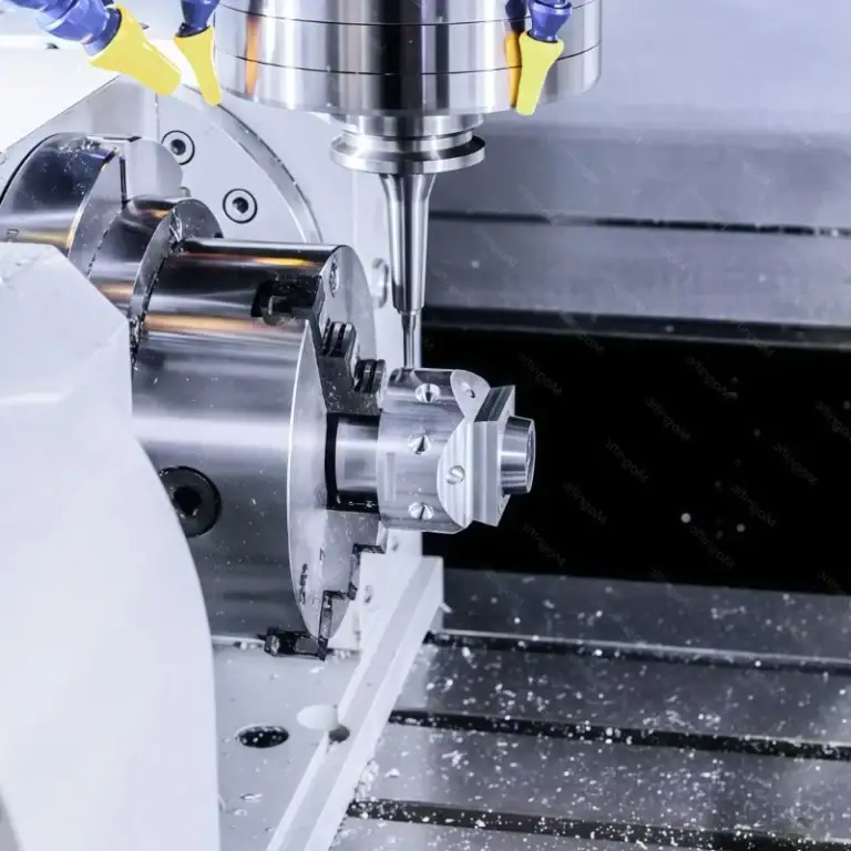
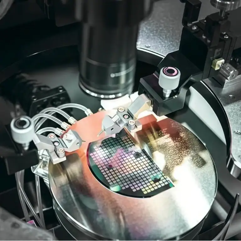
Semiconductor equipment requires highly precise components. Even a slightly misaligned hole or an uneven mounting surface can complicate assembly and affect equipment performance. Parts such as wafer handling components, vacuum connectors, precision mounting plates, and equipment supports often feature complex hole patterns, thin walls, and tight dimensional tolerances. Manufacturing these components involves much more than producing the correct shape. High-precision CNC machining enables custom parts to be manufactured directly from engineering drawings. With proper process planning and dimensional inspection, it helps reduce assembly rework and improve consistency from prototyping to assembly and batch production.
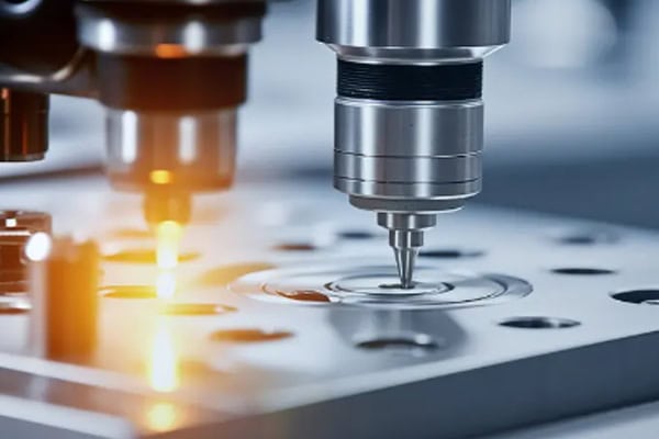
What Are the Main Challenges in High-Precision CNC Machining for Semiconductor Components?
For semiconductor components, meeting individual dimensional requirements is only the starting point. Hole spacing, mounting surface flatness, and the alignment of different interfaces are equally important. A part may pass individual dimensional checks but still fail to fit correctly during assembly because its machining datums or positional accuracy are not properly controlled. Identifying critical dimensions in advance and inspecting them during machining can help reduce assembly adjustments.
Precision Hole Positions and Mounting Dimensions Must Be Accurately Controlled
Mounting plates, locating blocks, and connectors used in semiconductor equipment often contain mounting holes, locating holes, and threaded holes. These features must align accurately with mating components, so machining cannot focus on hole diameter alone. Hole spacing and positional relationships also need careful control.
- Hole diameter and spacing: Dimensional deviations may make bolts difficult to install or cause connected components to become misaligned.
- Locating holes and threaded holes must meet drawing tolerances to avoid additional work such as enlarging holes or re-tapping threads during assembly.
- When several holes must align with one another, appropriate machining datums help reduce positioning errors between operations.
Keeping hole positions within the required tolerances makes assembly easier and reduces adjustment time. In particular, components with tight tolerances benefit from dimensional checks throughout the machining process.
Thin-Wall and Complex Structures Require Deformation Control
Some semiconductor components use thin walls, narrow slots, or hollowed-out structures to reduce weight or fit within limited equipment space. These designs have relatively low rigidity and can deform under clamping pressure or cutting forces. In some cases, dimensions appear correct during machining but change after the fixture is released.
For these components, clamping methods, cutting sequences, and machining allowances need careful planning rather than simply prioritizing speed.
- Position fixtures carefully to prevent excessive localized pressure.
- Machine thin-wall areas in stages to reduce deformation caused by heavy cuts.
- Leave an appropriate finishing allowance and gradually complete critical surfaces.
- Inspect dimensions after unclamping to confirm that the final geometry meets drawing requirements.
These process adjustments help improve dimensional stability, particularly for semiconductor components that require low weight, complex profiles, and accurate assembly.
Surface Quality and Deburring Are Equally Important
Even when a precision component meets its dimensional requirements, burrs around holes, residue along slot edges, or visible scratches may affect assembly and subsequent use. For semiconductor equipment parts, surface condition, cleanliness requirements, and drawing-specified surface roughness should all be included in the inspection process.
Deburring and cleaning should not be treated as minor finishing tasks. Defining surface requirements in advance and inspecting critical areas after machining can reduce additional work before delivery.
How Do CNC Machining Requirements Differ for Different Semiconductor Components?
Semiconductor equipment uses a wide range of components, and precision mounting plates, vacuum connectors, and engineering plastic parts have different structural and material characteristics. Machining processes should be planned around the actual application rather than using identical cutting parameters and inspection methods for every part. This approach helps maintain quality while avoiding unnecessary operations.
Precision Mounting Plates: Stable Flatness and Hole Alignment
Mounting plates provide positioning, support, and connection points. Their flatness and hole patterns directly affect equipment assembly. Machining must maintain the positional relationship between reference surfaces and holes, preventing situations where individual dimensions pass inspection but the completed part still fails to align properly.
- Flatness control: Uneven mounting surfaces may cause components to tilt or connections to become unstable.
- Hole spacing and positions must meet drawing tolerances to reduce the need for on-site hole correction.
- Threaded hole dimensions and depths must meet fastening requirements to ensure reliable connections.
For mounting plates with dense hole patterns, careful planning of machining sequences and inspection locations helps reduce errors caused by repeated positioning and makes it easier to assemble the parts with mating components.
Vacuum Connectors: Interfaces and Sealing Structures Are Critical
Vacuum-related components often include flanges, sealing grooves, through-holes, and threaded interfaces. Dimensional accuracy affects connection quality, while the surface condition of sealing areas also matters. Critical interfaces should receive focused inspection rather than relying on external dimensions alone.
- Sealing groove width and depth must meet design requirements to ensure proper seal installation.
- The positional relationship between flange surfaces and connection holes must be accurate to prevent assembly misalignment.
- Components with special requirements may need surface quality checks and leak testing when specified by the drawing or application.
The machining quality of vacuum connectors affects both assembly and sealing performance. Confirming critical interfaces and inspection requirements early can reduce rework and repeated machining.
Plastic and Metal Components Require Different Machining Parameters
Semiconductor equipment may use aluminum alloys, stainless steel, and engineering plastics. These materials behave differently during cutting, so tooling, machining parameters, and fixturing methods must be adjusted accordingly. Otherwise, problems such as burrs, poor surface quality, or dimensional changes may occur.
- Aluminum alloys: Focus on cutting stability, burr control around holes, and surface finish.
- Stainless steel requires attention to tool wear, cutting heat, and work hardening.
- Engineering plastics require controlled clamping force and machining temperature to prevent dimensional changes caused by deformation.
Adjusting the machining process to suit each material helps maintain dimensional accuracy and surface quality while supporting custom manufacturing for different semiconductor equipment designs.
| Component Type | CNC Machining Focus | Key Inspection Items |
| Precision Mounting Plate | Flatness, hole positions, threads | Flatness, hole spacing |
| Vacuum Connector | Flanges, sealing grooves, interfaces | Groove width, groove depth, interface dimensions |
| Thin-Wall Component | Fixturing, cutting sequence | Wall thickness, deformation |
| Engineering Plastic Part | Cutting parameters, clamping method | Dimensional changes, surface quality |
How Can Rework Be Reduced in High-Precision CNC Machining for Semiconductor Components?
Successful prototype machining does not automatically guarantee stable batch production. During continuous machining, tool wear, temperature changes, and fixturing conditions can affect component dimensions. If inspection is delayed until all parts are finished, an entire batch may already contain defects before the problem is discovered. Verifying critical dimensions, performing in-process inspections, and planning post-machining operations can make production more controllable.
Verify Critical Dimensions During Prototyping
The purpose of prototype machining is not simply to produce a part. It is also to verify whether the drawing requirements can be achieved in actual manufacturing. For semiconductor components that must fit with other parts, inspection reports should be supplemented by checks of hole positions, interfaces, and mounting structures.
- Check hole diameters, hole spacing, wall thickness, flatness, and drawing-specified tolerances.
- Verify locating holes, threaded holes, and connection interfaces to confirm accurate assembly positions.
- Inspect thin-wall components after unclamping to identify dimensional changes caused by deformation.
- Perform assembly verification early when the component must fit with other parts.
- Retain validated machining programs, fixturing methods, and inspection data for repeat production.
Problems identified during prototyping are generally easier to address than defects discovered after batch production. Confirming machining and acceptance requirements early also reduces repeated changes during later communication.
Monitor Critical Dimensions Throughout Batch Production
Batch CNC machining should not rely solely on inspecting the first part or waiting until the end of production. As machining continues, tool condition, machine temperature, and fixturing conditions may change, affecting critical dimensions.
- Inspect hole positions, mating dimensions, and mounting surfaces at appropriate intervals.
- When dimensions begin to drift, check tool wear and cutting parameters.
- Maintain inspection records for repeat orders to compare results between batches.
- Set suitable sampling frequencies according to the required tolerances to reduce the risk of batch-wide dimensional deviations.
In-process inspection helps identify problems early rather than waiting until every component has been completed. This is particularly valuable for semiconductor parts with demanding precision requirements and strict batch consistency expectations.
Deburring, Cleaning, and Inspection Must Not Be Skipped
After machining, small burrs or chips may remain around holes, threads, and narrow slots. If these residues are not removed, they may interfere with component fit and increase the amount of cleaning and assembly work required later. Post-processing should therefore be planned as part of the overall machining workflow.
- Remove burrs around holes, threads, and slot edges to prevent assembly interference.
- Inspect machined surfaces for scratches, impact marks, and visible defects.
- Remove chips and machining residue to prepare components for subsequent assembly.
- Maintain inspection records for critical dimensions to make machining results easier to verify.
| Inspection Item | What to Check | Main Purpose |
| Dimensional Tolerances | Length, thickness, hole diameter | Confirm compliance with drawings |
| Positional Accuracy | Hole spacing, hole positions, datum relationships | Ensure accurate assembly |
| Flatness | Mounting and locating surfaces | Reduce assembly deviations |
| Surface Quality | Burrs, scratches, surface roughness | Meet component requirements |
| Cleanliness | Chips and machining residue | Prepare parts for assembly |
What Are the Advantages of High-Precision CNC Machining for Semiconductor Components?
Semiconductor equipment components are frequently custom-made from engineering drawings. Some are standard mounting parts, while others contain deep holes, narrow slots, threads, and complex profiles. High-precision CNC machining uses programmed tool paths and planned manufacturing processes to accommodate different structures while controlling critical dimensions through inspection. These capabilities provide practical benefits for custom machining, prototype development, and repeat production.

Complex Structures Can Be Customized Directly from Drawings
Non-standard semiconductor components often have unique designs that cannot be met by fixed specifications. CNC machining allows programs and tool paths to be adjusted according to engineering drawings, accommodating different profiles, hole patterns, and connection structures.
- Complex profile machining: Suitable for special contours, non-standard supports, and custom connection structures.
- Deep holes, stepped holes, threaded holes, and narrow slots can be machined to drawing requirements.
- Multiple mounting and locating holes can be positioned using properly planned machining datums to reduce positional errors.
- When a component design changes, the machining program can be updated to accommodate revised dimensions and structures.
This flexibility is useful for customized semiconductor equipment development and allows different equipment models to use components designed for their specific requirements.
Critical Dimensions and Assembly Errors Can Be Better Controlled
High-precision CNC machining involves more than completing cutting operations. Critical dimensions must also be incorporated into a stable manufacturing process. Hole diameters, hole spacing, mating dimensions, and mounting surfaces can all be machined and inspected according to drawing tolerances.
- Critical dimensions can be controlled to specified tolerances, reducing rework caused by incorrect hole positions, diameters, or mating fits.
- Mounting surfaces, locating surfaces, and connection interfaces can receive dedicated machining and inspection.
- Validated processes can be reused for repeat production to reduce dimensional differences between batches.
- In-process inspection helps identify deviations before they accumulate and affect final delivery.
For semiconductor components that require accurate assembly, consistent dimensional control reduces on-site adjustments and helps parts move into subsequent assembly operations more smoothly.
Suitable for Prototypes, Small Batches, and Batch Production
During semiconductor equipment development, drawings may be revised several times, and production quantities often change as projects progress. CNC machining does not require a dedicated mold for every component design. Programs can be updated to accommodate different production requirements.
- Individual prototypes can be used to verify dimensions, structures, and assembly performance.
- Small-batch production suits projects with frequent design revisions or uncertain initial quantities.
- Validated machining programs and inspection requirements can be reused for repeat production.
- Machining parameters can be adjusted to suit different materials and component structures.
This production flexibility helps semiconductor equipment projects move from prototype verification to batch manufacturing while reducing additional preparation work caused by design changes.
Machining, Deburring, and Inspection Can Be Coordinated Efficiently
The final quality of precision components depends not only on cutting operations but also on post-processing and inspection. Coordinating these steps within a planned workflow helps prevent omissions before delivery.
- Schedule deburring and cleaning after machining to reduce additional assembly work.
- Inspect dimensions, tolerances, and surface conditions to confirm compliance with drawing requirements.
- Retain essential machining and inspection records for future verification and repeat production.
Semiconductor equipment demands high dimensional accuracy, reliable assembly, and consistent batch quality. High-precision CNC machining supports complex custom structures, critical dimensional control, and component development. Whether manufacturing precision mounting plates, vacuum connectors, or plastic and metal components, the machining process should suit the material, drawing tolerances, and intended application. TIRAPID provides CNC machining services for precision semiconductor components, with machining plans tailored to drawings, materials, and tolerance requirements, supporting both prototype development and batch production.