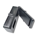
A wafer chuck is a precision holding device that supports and secures silicon wafers during semiconductor manufacturing, inspection, and testing. Depending on its design, it uses vacuum pressure, electrostatic attraction, or mechanical holding to keep wafers stable without excessive deformation. Flatness, surface cleanliness, thermal control, and material compatibility are critical because even small positioning errors or particles can affect processing accuracy and wafer quality.
This guide explains what a wafer chuck is, how different clamping technologies work, and which ceramic and metal materials are used in its construction.
What Is a Wafer Chuck and Why Is It Important?
A wafer chuck is a precision fixture that holds and supports semiconductor wafers during manufacturing or testing. It is important because stable wafer positioning, controlled flatness, temperature uniformity, and low contamination directly affect process repeatability and component quality. Vacuum, electrostatic, and mechanical chucking methods are selected according to the equipment environment and wafer-handling requirements.
How Wafer Chucks Hold and Position Silicon Wafers
Wafer chucks hold silicon wafers by applying a controlled force that prevents unwanted movement during processing. Vacuum systems use a pressure difference, electrostatic systems use electric fields, and mechanical systems apply force through selected contact features.
The holding force must be distributed appropriately across the wafer. Excessive local pressure can cause bending or damage, while insufficient holding force may allow movement during scanning, processing, or automated transfer.
A typical wafer chuck includes a support surface, holding mechanism, mounting interface, and optional lift pins or temperature-control features. The arrangement depends on whether the chuck operates in atmospheric conditions, vacuum equipment, or a specialized test environment.
Why Flatness, Thermal Stability, and Cleanliness Matter
Flatness matters because the chuck surface influences how evenly the wafer is supported. Poor surface geometry can introduce wafer deformation, unstable contact, or positioning errors during precision processing.
Thermal stability is equally important. Semiconductor processes may heat or cool the wafer, and temperature differences can cause expansion, thermal distortion, or inconsistent process conditions. The chuck must provide the required thermal behavior without introducing unwanted movement.
Cleanliness protects the wafer from particles, residues, and contamination originating from the supporting surface. Effective wafer care involves compatible materials, cleanable geometry, appropriate handling, and qualified cleaning procedures rather than simply producing a polished appearance.
Wafer Chucks vs. Chuck Tables
A wafer chuck is the wafer-holding component, while a chuck table generally refers to a supporting worktable or stage incorporating a holding surface. However, semiconductor equipment manufacturers sometimes use these terms interchangeably.
The distinction is therefore functional rather than universal. A chuck table may contain vacuum grooves, support pins, or an integrated chucking mechanism, while a wafer chuck may be installed as part of a larger positioning assembly.
Engineers should identify the actual mechanical and functional requirements instead of relying only on the component name.
| Feature | Wafer Chuck | Chuck Table |
| Main function | Holds and supports the wafer | Provides a workholding or positioning platform |
| Typical structure | Vacuum, electrostatic, or mechanical holding surface | Table or stage with integrated holding features |
| Common applications | Processing, inspection, and testing | Processing, dicing, grinding, and positioning |
| Important requirements | Clamping behavior, flatness, contamination control | Flatness, mounting accuracy, positioning |
| Terminology | Often refers to the holding component | May overlap with wafer chuck terminology |
What Are the Main Types of Wafer Chucks?
The main types of wafer chucks are electrostatic chucks, vacuum chucks, and mechanical or hybrid chucks. Electrostatic chucks use an electric field to secure wafers, vacuum chucks use differential pressure, and mechanical systems use controlled contact forces. Each design provides different advantages for holding stability, operating environment, temperature control, and wafer release.
Electrostatic Wafer Chucks and Their Working Principles
An electrostatic wafer chuck uses electrodes beneath a dielectric surface to generate electrostatic attraction between the chuck and wafer. This holding method is widely used in semiconductor plasma processing and other controlled environments.
In electrostatic chuck semiconductor applications, a power supply energizes the embedded electrodes. The resulting electric field produces holding force, while controlled electrical discharge and release procedures allow the wafer to be removed after processing.
Two important mechanisms are Coulombic attraction and the Johnsen–Rahbek effect. Their behavior depends on dielectric properties, interface conditions, electrical resistance, and operating parameters. Electrostatic chucking can work in vacuum chambers where conventional pressure-differential vacuum holding is ineffective.
Vacuum Wafer Chucks and Porous Vacuum Designs
Vacuum wafer chucks hold wafers by reducing pressure beneath selected areas of the wafer, allowing the higher surrounding pressure to press the wafer against the chuck surface. This approach is common in atmospheric inspection, testing, grinding, and other suitable operations.
Conventional designs use grooves and vacuum holes connected to internal distribution channels. A silicon wafer vacuum chuck may incorporate concentric grooves, radial channels, and controlled support areas to provide suitable holding force and stability.
Porous vacuum designs distribute suction through interconnected pores rather than relying entirely on discrete openings. A properly designed porous surface can improve pressure distribution, but its performance depends on permeability, sealing, wafer flatness, and system airflow.
Mechanical Edge-Grip and Hybrid Chucks
Mechanical wafer chucks use edge clamps, fingers, support pins, or other controlled contact features to hold a wafer. They are useful when the application does not permit conventional vacuum or electrostatic holding.
Edge-grip systems are often considered when backside access, special wafer surfaces, or transfer requirements make face contact undesirable. However, edge contact introduces local mechanical loads and must be designed to avoid chipping or excessive bending.
Hybrid solutions combine different holding or support methods. A bernoulli wafer chuck, for example, uses controlled gas flow to create an aerodynamic holding effect with reduced direct surface contact in suitable handling conditions. Gas cleanliness, flow stability, and wafer control remain essential.
| Wafer Chuck Type | Holding Principle | Common Applications | Main Limitation |
| Electrostatic | Electric-field attraction | Plasma processing and selected vacuum equipment | Electrical control and release complexity |
| Vacuum | Pressure differential | Inspection, probing, and atmospheric processing | Requires suitable pressure difference and sealing |
| Porous Vacuum | Distributed suction through porous media | Thin-wafer support and precision handling | Pore contamination and permeability control |
| Mechanical Edge-Grip | Physical edge contact | Selected transfer, testing, and handling operations | Local edge stress |
| Bernoulli | Aerodynamic pressure effect | Specialized wafer transfer and handling | Gas supply, clearance, and particle-control requirements |
What Materials Are Used to Make Wafer Chucks?
Wafer chucks are manufactured from advanced ceramics, aluminum alloys, stainless steel, and engineered multi-material assemblies. Alumina and aluminum nitride are widely used in electrostatic and thermal applications, while silicon carbide and porous ceramics support selected precision holding designs. Metal components commonly provide structural support, mounting interfaces, and internal cooling or vacuum channels.

Alumina and Aluminum Nitride Ceramics
Alumina, or aluminum oxide (Al₂O₃), is commonly used for ceramic wafer chucks because it offers high hardness, electrical insulation, wear resistance, and useful dimensional stability. It can provide a durable support surface when appropriately processed.
Aluminum nitride (AlN) offers higher thermal conductivity than conventional alumina grades and is frequently selected for applications requiring efficient heat transfer. Its electrical properties can also be engineered for different electrostatic chuck designs.
Both materials require specialized manufacturing methods. Their hardness and brittleness make conventional metal-cutting strategies unsuitable for many finishing operations, while precision grinding and lapping may be necessary to achieve the required geometry.
Silicon Carbide and Porous Ceramic Materials
Silicon carbide provides high stiffness, wear resistance, thermal stability, and useful thermal conductivity. A silicon carbide wafer chuck may be selected for precision support or challenging equipment environments where these properties are valuable.
However, silicon carbide properties vary with composition and manufacturing method. Electrical conductivity, porosity, purity, and chemical resistance must be checked for the specific grade rather than assumed from the material name.
Porous ceramic materials are used in selected vacuum chuck designs to distribute suction across the contact surface. The pore structure influences airflow, support uniformity, contamination behavior, and cleaning requirements.
A porous ceramic material may be based on alumina, silicon carbide, or another suitable composition. Material selection must consider both the properties of the ceramic and the function of the complete vacuum system.
Aluminum, Stainless Steel, and Metal-Ceramic Assemblies
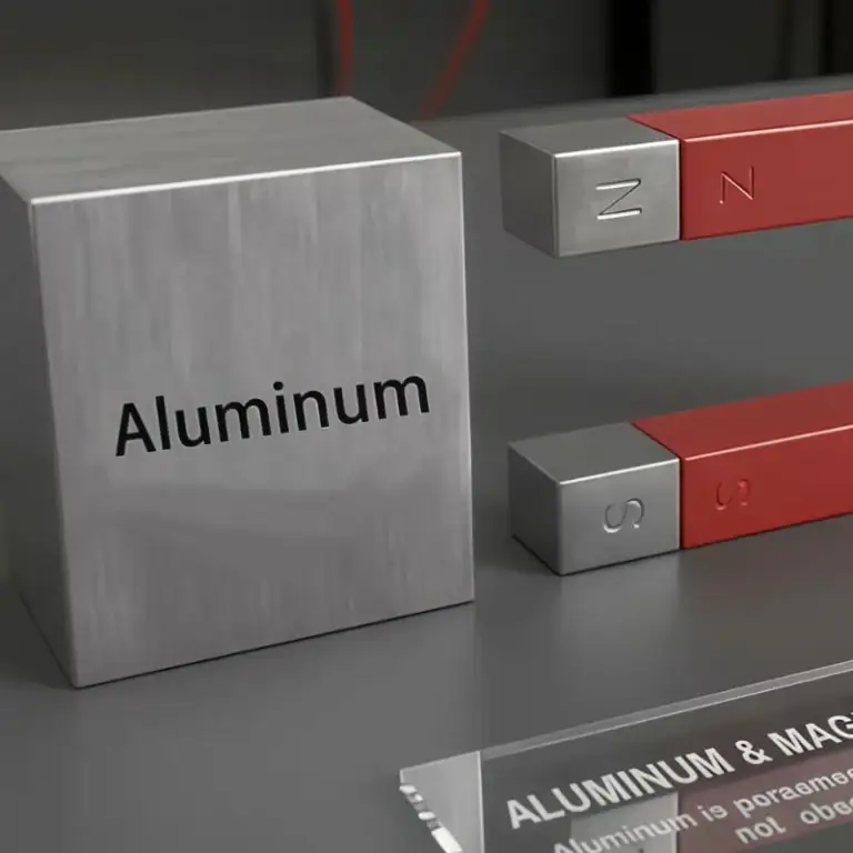
Aluminum alloys are widely used for wafer chuck bases and supporting components because they offer relatively low weight, good machinability, and useful thermal conductivity. CNC machining can create mounting holes, vacuum distribution channels, pockets, and precision interfaces.
Stainless steel may be selected for structural features, fasteners, or components requiring particular corrosion resistance and mechanical properties. Its suitability depends on process chemistry, cleanliness requirements, and thermal expansion.
Many advanced wafer chucks use metal-ceramic assemblies. The ceramic provides the required electrical or wafer-contact behavior, while a machined metal base supports the structure and accommodates cooling or mounting features.
| Material | Main Advantages | Common Function | Main Consideration |
| Alumina | Hardness, electrical insulation, wear resistance | Ceramic support and dielectric surfaces | Brittle machining behavior |
| Aluminum Nitride | High thermal conductivity, engineered electrical properties | Thermal and electrostatic systems | Grade-specific electrical behavior |
| Silicon Carbide | High stiffness, thermal stability, wear resistance | Precision support surfaces | Grade and conductivity selection |
| Porous Ceramic | Distributed vacuum flow | Vacuum holding surfaces | Pore consistency and cleaning |
| Aluminum Alloy | Machinability, low weight, thermal conductivity | Bases and channel structures | Thermal expansion and surface treatment |
| Stainless Steel | Mechanical strength and selected corrosion resistance | Supports and hardware | Weight and thermal behavior |
What Are the Key Wafer Chuck Design Features and Specifications?
The key wafer chuck specifications include wafer size, supporting geometry, flatness, surface roughness, clamping force, vacuum pressure, thermal performance, electrical properties, and cleanliness. These parameters determine how effectively the chuck supports the wafer during processing. The required values must be established according to the application rather than applying a single universal tolerance or pressure specification.
Wafer Sizes, Chuck Geometry, and Mounting Features
Wafer chuck geometry is selected according to the wafer diameter, thickness, allowable contact regions, and equipment configuration. Common semiconductor wafer diameters include 150 mm, 200 mm, and 300 mm, although other substrate sizes are also used.
A chuck must provide adequate wafer support while accommodating lift pins, vacuum connections, electrical interfaces, or thermal management features when required. The layout should prevent interference with surrounding equipment.
Mounting surfaces and locating features are especially important for repeatability. Precision CNC machining can produce metal bases with accurately positioned mounting holes, reference surfaces, and fluid channels that support assembly alignment.
Flatness, Surface Roughness, and Contact Uniformity
Flatness describes the geometric variation of a surface from an ideal plane. Surface roughness describes smaller-scale surface texture. Both affect wafer support but represent different inspection requirements.
Wafer chuck flatness may be specified in micrometers, particularly for demanding positioning or optical applications. The actual tolerance depends on wafer size, process requirements, temperature, and the complete stage design.
Contact uniformity depends on the surface pattern, support distribution, and wafer condition. A surface that is polished to a very low roughness value is not automatically suitable if its geometry, contact pattern, or release behavior is incorrect.
Clamping Force, Vacuum Pressure, and Release Control
Clamping force must be sufficient to resist process loads without damaging or excessively deforming the wafer. For vacuum systems, the ideal holding force depends on pressure difference and effective sealed area.
The simplified relationship is:
Holding Force = Pressure Difference × Effective Vacuum Area
For example, assume a 200 mm wafer is held under an illustrative pressure difference of 20 kPa, with an effective sealed area equal to 50% of the wafer’s circular area.
- Wafer diameter: 200 mm
- Wafer area: approximately 0.0314 m²
- Effective vacuum area: approximately 0.0157 m²
- Pressure difference: 20,000 Pa
- Ideal holding force: approximately 314 N
This calculation is a simplified theoretical estimate, not a recommended operating setting. Actual holding force may be lower because of leakage, wafer curvature, support geometry, and pressure losses. Release performance must also be evaluated to prevent sticking or wafer damage.
Thermal Management, Electrical Properties, and Particle Control
Thermal management controls wafer temperature and limits unwanted expansion during processing. Some electrostatic chucks incorporate heating, cooling, or backside gas systems to support controlled thermal conditions.
Electrical properties are essential for electrostatic chucks because dielectric behavior, leakage current, and electrical breakdown characteristics affect holding performance and release reliability.
Contamination control requires suitable materials, cleanable surfaces, controlled processing, and compatible assembly methods. Even a geometrically accurate chuck may be unsuitable for semiconductor service if particles or residues are introduced during manufacturing.
| Design Parameter | Main Purpose | Typical Engineering Unit |
| Wafer diameter | Equipment compatibility | mm |
| Surface flatness | Support geometry | µm |
| Surface roughness | Contact texture | µm Ra or other specified parameter |
| Vacuum pressure differential | Holding force | kPa |
| Electrostatic voltage | Electric-field control | V |
| Thermal uniformity | Temperature distribution | °C or K |
| Electrical resistivity | Dielectric or conduction behavior | Ω·cm |
| Particle performance | Cleanliness verification | Particle counts by size and area |
| Mounting accuracy | Assembly alignment | mm or µm |
How Are Precision Wafer Chuck Components Manufactured?
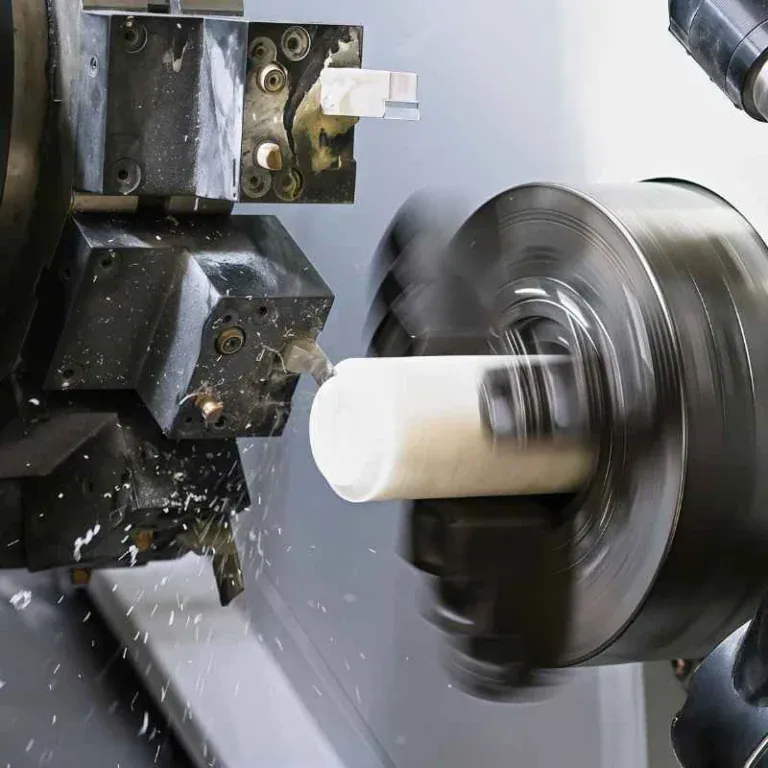
Precision wafer chuck components are manufactured through material preparation, CNC machining, specialized ceramic processing, finishing, assembly, and inspection. CNC milling and drilling are especially useful for metal bases, mounting interfaces, and vacuum channels. Ceramic support surfaces usually require material-specific shaping, grinding, lapping, or polishing to achieve the necessary flatness and surface condition.
| Manufacturing Stage | Typical Operation | Quality Objective |
| Material preparation | Verify alloy or ceramic grade | Material suitability |
| CNC machining | Produce metal geometry and channels | Dimensional accuracy |
| Ceramic processing | Shape and finish ceramic components | Geometry and surface integrity |
| Surface finishing | Grinding, lapping, or polishing | Flatness and controlled texture |
| Assembly | Join structural and functional components | Alignment and integrity |
| Inspection | Dimensional and functional verification | Specification compliance |
| Cleaning | Remove manufacturing contamination | Process cleanliness |
CNC Machining of Metal Bases and Vacuum Channels
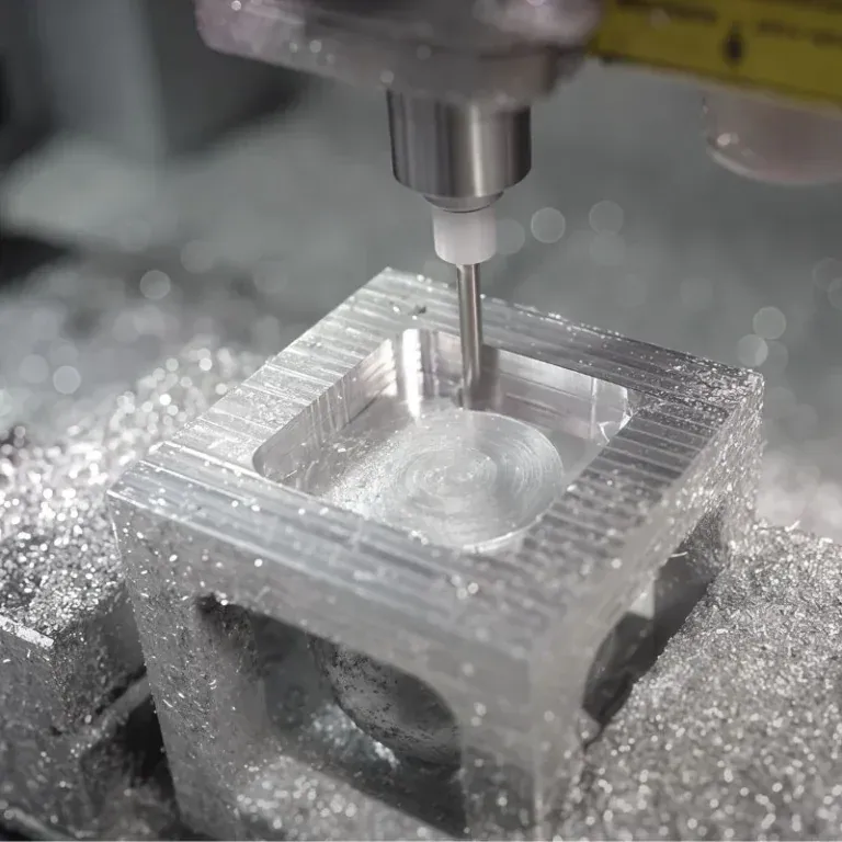
CNC machining produces wafer chuck metal bases, support plates, mounting structures, and vacuum distribution features. Aluminum and stainless steel components may require precise holes, pockets, channels, and accurately located assembly interfaces.
Vacuum channels must be designed to provide suitable flow distribution without weakening the supporting structure. Groove dimensions, channel connections, sealing regions, and surface intersections all influence the final holding performance.
Machining sequence is important for flatness control. A large thin plate may distort when material is removed unevenly, requiring appropriate fixturing, balanced machining, and finishing operations.
Precision Grinding, Lapping, and Polishing of Ceramic Surfaces
Ceramic wafer chuck surfaces are often finished through grinding, lapping, and polishing rather than conventional metal-style milling alone. These processes are used to control thickness, flatness, parallelism, and surface texture.
Grinding uses suitable abrasives to remove material from hard ceramic surfaces. Lapping can improve flatness through controlled abrasive contact, while polishing may further refine texture where the application requires it.
Excessive grinding force or unsuitable abrasive conditions can produce cracks, edge chipping, or subsurface damage. The finishing method must therefore match the ceramic grade and required wafer-contact condition.
Assembly, Dimensional Inspection, and Cleanliness Verification
Wafer chuck assembly combines the supporting structure, holding surface, and functional interfaces into a complete component. Depending on the design, these may include vacuum connections, ceramic layers, lift-pin arrangements, or temperature-control features.
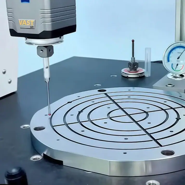
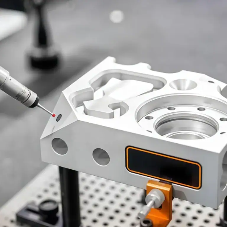
Dimensional inspection verifies critical mounting features, flatness, parallelism, hole positions, and contact-surface geometry. Coordinate measuring machines, surface measurement systems, and suitable optical instruments may be used.
Cleanliness verification is also important because machining fluids, abrasive particles, metal debris, and handling residues can affect semiconductor service. Final cleaning methods and acceptance criteria must be compatible with the material and intended environment.
Where Are Wafer Chucks Used in Semiconductor Manufacturing?
Wafer chucks are used in semiconductor etching, thin-film deposition, lithography, wafer probing, inspection, testing, and automated handling equipment. Their primary function is to maintain stable wafer support while meeting the specific positioning, thermal, electrical, and cleanliness requirements of each process. Different manufacturing stages require different chuck technologies.

Etching and Thin-Film Deposition
Etching equipment uses wafer chucks to hold substrates during processes that remove selected material from the wafer surface. Electrostatic chucks are common in many plasma etching systems because they can maintain holding force in vacuum environments.
Thin-film deposition processes may also require stable wafer positioning and temperature control. Some systems use electrostatic chucks, heated susceptors, or specialized support platforms according to process chemistry and equipment design.
The chuck material must be compatible with the operating environment. Plasma exposure, electrical bias, temperature cycling, and particle generation can all influence material selection and surface design.
Lithography and Precision Wafer Positioning
Lithography equipment requires accurate wafer positioning and surface control so patterns can be transferred with the required alignment and focus. The wafer support system must minimize unwanted movement and deformation.
Vacuum or other specialized holding technologies may be used depending on the equipment architecture. The supporting stage and chuck must work together to control positional stability, flatness, and thermal effects.
Mechanical interfaces are important because alignment errors can originate outside the wafer-contact surface. Mounting features, reference surfaces, and motion-stage connections must therefore be manufactured and inspected appropriately.
Wafer Probing, Inspection, and Testing
Wafer probing equipment uses a chuck to position the wafer beneath test probes that contact designated electrical features. The chuck must support repeatable movement while maintaining appropriate thermal and mechanical stability.
A thermal chuck may incorporate a temperature-controlled hot cold plate or another heating and cooling arrangement for electrical testing under defined conditions. The actual operating range depends on the system design.
Inspection equipment may use vacuum support to secure wafers during optical measurement, metrology, or defect detection. Flatness, vibration control, and contamination management are important for obtaining consistent measurement results.
Automated Wafer Handling and Transfer
Automated wafer-handling systems move substrates between equipment modules using robotic arms, end effectors, and specialized holding devices. The selected support method must prevent slipping, scratching, and excessive mechanical stress.
Vacuum holding is useful in suitable atmospheric transfer systems, while edge-grip or aerodynamic handling may be preferred for applications requiring reduced surface contact.
Transfer components must also support controlled wafer release. A system that holds securely but releases inconsistently can cause positioning errors, equipment interruptions, or wafer damage.
| Application | Common Holding Approach | Main Engineering Requirement |
| Plasma etching | Electrostatic | Vacuum compatibility and thermal control |
| Selected deposition equipment | Electrostatic or specialized support | Temperature and process compatibility |
| Lithography | Vacuum or specialized precision support | Positioning and flatness |
| Electrical probing | Vacuum or thermal chuck | Stable contact and controlled temperature |
| Optical inspection | Vacuum or precision support | Flatness and repeatability |
| Automated transfer | Vacuum, edge-grip, or aerodynamic | Reliable handling and release |
What Problems Affect Wafer Chuck Performance and Reliability?
Common wafer chuck problems include uneven clamping, wafer slippage, warpage, thermal drift, particle contamination, electrostatic release failure, and surface wear. These issues can result from incorrect holding force, unstable temperature, damaged contact surfaces, blocked vacuum channels, or unsuitable materials. Reliable operation requires both correct design and controlled maintenance.
Uneven Clamping, Wafer Slippage, and Warpage
Uneven clamping occurs when holding force is distributed poorly across the wafer. Possible causes include blocked vacuum holes, leaks, inconsistent support geometry, or electrostatic performance variation.
Wafer slippage may occur if the available holding force is insufficient for handling acceleration or process loading. Increasing force without checking wafer strength and contact conditions can create new damage risks.
Warpage may originate in the wafer itself or develop because of nonuniform support. Engineers should evaluate wafer bow, chuck geometry, holding distribution, and the operating environment before changing the design.
Thermal Drift and Particle Contamination
Thermal drift occurs when temperature changes alter the dimensions or position of the chuck, wafer, or supporting equipment. Different materials can expand by different amounts, creating additional stresses in mixed-material assemblies.
For example, a 300 mm aluminum component with a thermal expansion coefficient of approximately 23 × 10⁻⁶/K would expand by about 6.9 µm for a uniform 1°C temperature increase under a simplified unconstrained model.
Particle contamination can originate from surface wear, cleaning residues, handling, or process deposits. It may interfere with wafer support or create defects. Cleaning procedures should remove contamination without damaging coatings, porous surfaces, or electrical structures.
Electrostatic Release Issues and Surface Wear
Electrostatic release problems occur when residual charge or unsuitable electrical control prevents the wafer from separating as expected. The behavior depends on chuck design, dielectric properties, surface conditions, and discharge procedures.
Surface wear may develop through repeated wafer contact, process exposure, or maintenance operations. Changes in surface texture or support patterns can affect clamping performance and contamination levels.
The response should address the specific mechanism. Electrical release problems require appropriate system diagnosis, while damaged contact geometry may require inspection, qualified refurbishment, or component replacement.
| Performance Problem | Possible Cause | Engineering Response |
| Weak vacuum holding | Leakage or blocked channels | Check pressure distribution and flow |
| Wafer slippage | Insufficient holding force | Review loading and clamping conditions |
| Wafer warpage | Uneven support or pre-existing bow | Evaluate support geometry and wafer condition |
| Thermal drift | Temperature instability | Improve thermal management |
| Particle contamination | Wear or residual debris | Apply compatible cleaning and inspection |
| Delayed electrostatic release | Residual charge or control problems | Verify discharge and release system |
| Surface degradation | Process exposure or repeated contact | Inspect surface and assess refurbishment |
How Do You Choose the Right Wafer Chuck?
The right wafer chuck should be selected according to process environment, holding method, wafer size, material compatibility, flatness requirements, temperature control, cleanliness, maintenance, and total operating cost. Vacuum chucks are suitable for many atmospheric applications, while electrostatic chucks are often preferred in vacuum plasma processing. Material and structural design must support the required function without introducing unnecessary complexity.
Selecting the Clamping Method for Different Process Environments
The process environment is the first major selection factor. Conventional vacuum chucking requires a sufficient pressure difference across the wafer and therefore cannot be assumed to provide effective holding in a fully evacuated chamber.
Electrostatic holding is useful for selected vacuum processing systems, although it requires appropriate electrical control, dielectric properties, and release procedures.
Mechanical edge-grip or aerodynamic methods may be considered for transfer operations where contact restrictions or special wafer surfaces limit conventional holding choices.
Matching Materials, Wafer Size, and Precision Requirements
The selected material must match the operating temperature, electrical requirements, chemical exposure, cleanliness expectations, and mechanical design. Alumina, aluminum nitride, silicon carbide, and metal alloys offer different performance advantages.
Wafer diameter and thickness determine the support geometry and handling approach. Larger or thinner substrates may require additional attention to bending, local contact pressure, and distributed support.
Precision requirements must also be expressed clearly. Flatness, parallelism, roughness, mounting accuracy, and thermal uniformity should be evaluated separately because one specification does not guarantee the others.
Key Selection Considerations
- Process Environment:Atmospheric, vacuum, plasma, or specialized testing conditions.
- Clamping Method:Vacuum, electrostatic, mechanical, or hybrid holding.
- Material Compatibility:Thermal, electrical, chemical, and wear requirements.
- Wafer Geometry:Diameter, thickness, bow, and allowable contact regions.
- Precision Requirements:Flatness, surface texture, positioning, and thermal uniformity.
- Maintenance:Cleaning access, surface life, release reliability, and service requirements.
Evaluating Maintenance, Service Life, and Total Cost
Wafer chuck cost includes more than the initial manufacturing price. Maintenance, cleaning, replacement parts, operating utilities, process downtime, and inspection requirements contribute to total ownership cost.
A simpler vacuum chuck may be economical for appropriate atmospheric equipment, while a specialized electrostatic system may be necessary for vacuum plasma applications.
Manufacturing cost also depends on material, geometry, processing sequence, and quality requirements. Precision CNC-machined metal bases can involve complex channels and tight mounting tolerances, while ceramic components may require specialized grinding and finishing.
| Selection Factor | Main Engineering Question | Practical Decision |
| Environment | Does the process operate in vacuum? | Evaluate electrostatic or compatible alternatives |
| Wafer condition | Is the wafer thin, bowed, or fragile? | Review support and contact distribution |
| Temperature | Is active thermal control required? | Select compatible thermal architecture |
| Flatness | How much geometric variation is permitted? | Define measurable acceptance limits |
| Cleanliness | What particle limits apply? | Specify materials and cleaning requirements |
| Manufacturing | Which components require CNC machining or ceramic finishing? | Match process to material |
| Maintenance | Can the chuck be cleaned and serviced? | Review service life and operating cost |
What Are the Latest Trends in Wafer Chuck Technology?
Wafer chuck technology is advancing toward more precise thermal management, improved clamping uniformity, lower particle generation, specialized ceramic materials, and better process monitoring. These developments support increasingly demanding semiconductor equipment requirements, particularly where wafer positioning, temperature consistency, and reliable handling must be maintained over repeated operating cycles.

Advanced Temperature and Clamping Control
Advanced wafer chuck systems may combine multi-zone temperature control, improved backside gas management, and more sophisticated electrical clamping strategies.
These features help compensate for differences in heat generation and thermal contact across the wafer. Depending on the equipment, feedback from temperature, pressure, or electrical monitoring can support more consistent operation.
Reliable release is also an important development area. Controlled de-chucking reduces the risk of residual holding force, unexpected wafer movement, and handling interruptions.
New Ceramic Materials and Intelligent Process Monitoring
Advanced ceramic development focuses on improving thermal properties, electrical behavior, durability, cleanliness, and compatibility with demanding processing environments.
Material engineering may involve high-purity alumina, specialized aluminum nitride grades, silicon carbide, tailored coatings, and controlled porous structures. Each material must be qualified for its intended function.
Process monitoring can track relevant parameters such as vacuum pressure, gas flow, temperature, leakage current, and operating cycles. These measurements can help identify abnormal behavior before it causes wafer damage or equipment downtime.
FAQs
How Much Vacuum For Wafer Chuck?
The required vacuum depends on wafer diameter, effective sealed area, wafer bow, handling acceleration, and allowable deformation. Vacuum holding force can be estimated as the pressure difference multiplied by the effective area. For a 200 mm wafer with 0.0157 m² of effective area and a 20 kPa pressure difference, the ideal force is approximately 314 N. This is an illustrative calculation, not a recommended operating setting. Actual requirements must account for leakage, wafer strength, contact geometry, and process conditions.
Where Are Edge Grip Wafer Chuck Used?
Edge-grip wafer chucks are used in selected wafer transfer, inspection, bonding, testing, and specialized handling applications where backside access or reduced surface contact is important. Instead of supporting the wafer through a full-area vacuum surface, they hold it through controlled contact at designated edge locations. This can improve access to selected wafer surfaces, but it also creates localized mechanical loading. Engineers must evaluate edge condition, wafer thickness, clamping force, particle generation, and movement stability before selecting this approach.
What Are The Advantages Of Ceramic Wafer Chucks Over Metal Ones?
Ceramic wafer chucks can offer higher hardness, useful electrical insulation, good thermal stability, and improved resistance to certain process environments compared with conventional metal designs. Alumina is commonly used for insulating support surfaces, while aluminum nitride can provide higher thermal conductivity. However, ceramics are more brittle and often require specialized grinding or lapping. Metals remain useful for structural bases, cooling channels, and mounting interfaces. The better material depends on temperature, electrical behavior, cleanliness, mechanical loading, and manufacturing cost.
Can Ceramic Wafer Chucks Be Customized?
Yes. Ceramic wafer chucks can be customized for wafer diameter, thickness, flatness, groove layout, porosity, mounting interfaces, and selected electrical or thermal functions. Common wafer sizes include 150 mm, 200 mm, and 300 mm, although specialized substrates may require different dimensions. Customization may involve ceramic shaping, precision grinding, lapping, and integration with CNC-machined metal bases. Feasibility depends on material grade, feature geometry, manufacturing method, and inspection capability. Critical requirements should be confirmed through engineering review and process validation.
Conclusion
Wafer chucks are essential precision components that support stable semiconductor wafer processing, inspection, and handling. Vacuum, electrostatic, and mechanical designs offer different advantages depending on operating pressure, temperature, cleanliness, and positioning requirements. Material selection, surface flatness, contact geometry, thermal performance, and reliable release all influence chuck performance.
At TiRapid, we provide precision CNC machining and manufacturing services for custom semiconductor equipment components. Our team supports precision metal bases, mounting features, vacuum channels, DFM analysis, surface finishing, and dimensional inspection to help customers produce accurate, reliable, and application-ready parts.