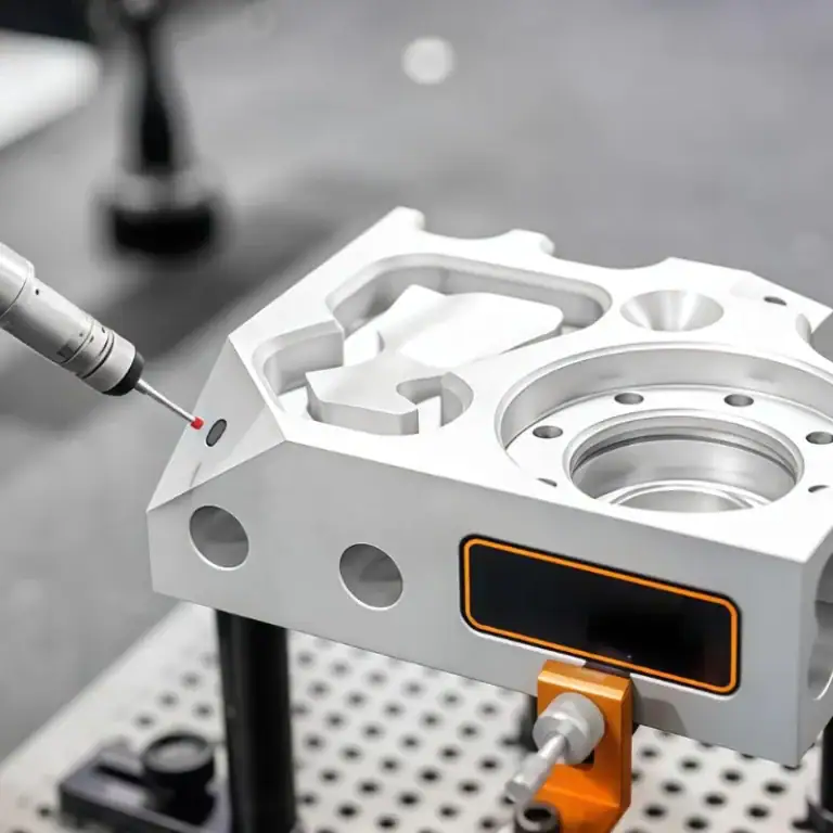
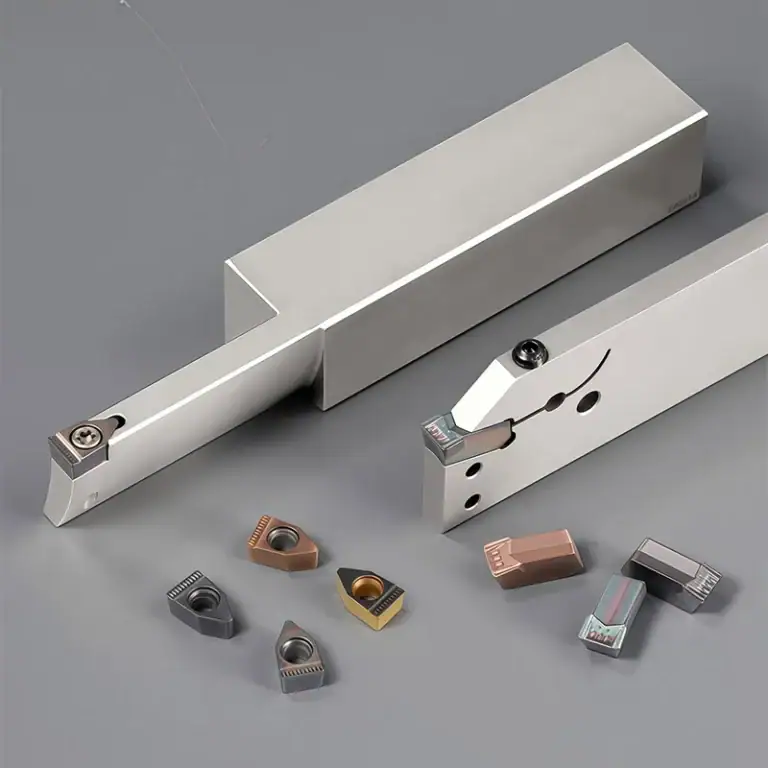
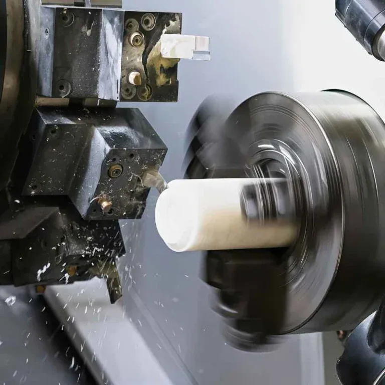
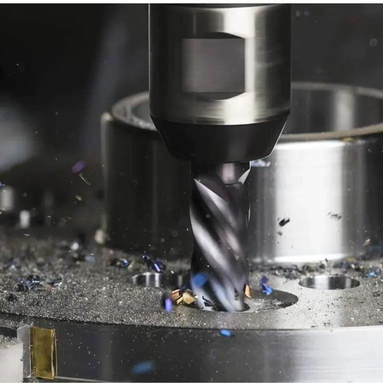
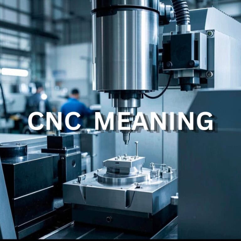
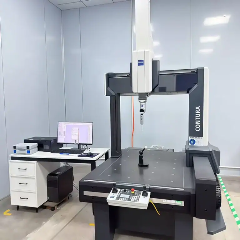
In semiconductor manufacturing equipment, some components may be small in size but play a critical role in equipment stability and production efficiency. As semiconductor processes continue to advance, internal equipment parts must withstand challenging conditions such as high temperatures, vacuum environments, chemical corrosion, and strict cleanliness requirements. PEEK, as a high-performance engineering plastic, has become widely used in semiconductor equipment components such as insulation parts, wafer positioning components, and vacuum system parts due to its excellent heat resistance, corrosion resistance, high strength, and dimensional stability. However, the better the material performance, the higher the machining requirements. Professional CNC machining technology is required to achieve stable and high-precision PEEK component manufacturing for semiconductor applications.
Why Is PEEK Component Machining Increasingly Important in the Semiconductor Industry?
Semiconductor equipment has extremely strict requirements for material performance and machining quality. During operation, many internal components are exposed to high temperatures, chemical media, and vacuum conditions. If the material performance is unstable, it may cause deformation, wear, or reduced equipment accuracy. Although PEEK is classified as a plastic material, it offers comprehensive performance comparable to some metal materials and provides significant advantages in demanding applications. At the same time, semiconductor manufacturing requires strict control over dimensional accuracy, surface quality, and cleanliness, driving the development of advanced PEEK component machining technologies.

PEEK Material Properties Meet Semiconductor Equipment Requirements
PEEK is a high-performance engineering plastic with excellent thermal resistance, chemical resistance, and mechanical strength. Compared with standard engineering plastics, PEEK maintains better stability in harsh environments and is suitable for manufacturing critical semiconductor equipment components.
- Strong high-temperature resistance, allowing components to maintain performance in high-temperature operating environments and reducing material degradation during long-term use.
- Excellent chemical corrosion resistance, enabling stable performance when exposed to cleaning agents, gases, and chemical media.
- Good electrical insulation properties, making it suitable for electrical isolation components inside semiconductor equipment.
- High dimensional stability, with low moisture absorption helping reduce size changes caused by environmental variations.
These material advantages make PEEK an increasingly common choice for semiconductor equipment manufacturing and create greater demand for high-performance plastic component machining.
Semiconductor Components Require Higher Machining Accuracy
Although PEEK components are often small, they usually perform important functions within semiconductor equipment. Components such as wafer supports, positioning structures, and vacuum system parts require precise matching with other equipment assemblies.
- Control dimensional tolerances, ensuring accurate installation positions and proper component fitting to prevent operational issues.
- Improve surface machining quality, reducing burrs, scratches, and machining residues that may affect clean semiconductor environments.
- Maintain batch-to-batch consistency, ensuring different production batches achieve the same performance standards for long-term equipment maintenance.
For semiconductor manufacturers, PEEK machining is not only about meeting drawing specifications but also about ensuring stable performance throughout long-term operation.
What Are the Challenges of CNC Machining PEEK Components?
Many customers initially assume that PEEK components are easier to manufacture because they are plastic rather than metal. However, this is not always the case. PEEK has high toughness and wear resistance, which can create challenges during machining, including tool selection, dimensional control, and surface finish management. If machining parameters are not properly adjusted, problems such as dimensional deviation, poor surface quality, or component failure may occur. Producing PEEK components that meet semiconductor equipment standards requires a deep understanding of material characteristics and professional CNC machining processes.
Material Elasticity Affects Dimensional Control
Unlike brittle materials, PEEK has certain flexibility and may experience elastic deformation during machining. This becomes more noticeable when manufacturing thin-wall components or parts with strict dimensional requirements.
- Control cutting forces properly, preventing excessive machining pressure from causing deformation and affecting final accuracy.
- Optimize machining sequences, reducing the impact of internal material stress through proper roughing and finishing processes.
- Strengthen critical dimension inspections, identifying machining changes early and ensuring components meet design requirements.
A scientific CNC machining process can effectively reduce deformation risks and improve the dimensional stability of PEEK components.
Tool Selection and Machining Parameters Affect Results
Although PEEK is a plastic material, its wear resistance is relatively high. Improper tooling selection may reduce machining efficiency or create unstable surface quality. For semiconductor components, surface conditions are especially important, making tool management and parameter control essential.
- Select sharp cutting tools suitable for PEEK machining, reducing friction and improving machining performance.
- Adjust cutting parameters properly, controlling heat generation and preventing dimensional changes.
- Optimize machining paths according to component structures, reducing unnecessary cutting stress and improving stability.
The right tooling strategy helps reduce machining defects while improving overall PEEK component production efficiency.
Surface Quality Directly Impacts Semiconductor Applications
Semiconductor equipment requires extremely clean operating environments. If PEEK components contain burrs, particles, or machining defects, they may affect equipment performance and manufacturing stability.
- Reduce machining burrs and surface damage, improving component appearance and functional performance.
- Control component cleanliness, minimizing the impact of machining residues.
- Improve surface consistency, meeting the requirements of long-term semiconductor equipment operation.
Good surface quality control allows PEEK components to better meet the needs of advanced semiconductor manufacturing equipment.
How Does CNC Machining Improve PEEK Semiconductor Component Manufacturing?
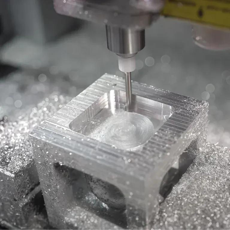
As semiconductor equipment continues to evolve, component designs are becoming increasingly complex, creating higher demands for PEEK machining capabilities. Different equipment parts focus on different performance requirements. Some components require extremely high dimensional accuracy, some require excellent insulation performance, while others must withstand vacuum environments. During actual production, machining solutions need to be developed according to component applications. With advantages such as digital control, high repeatability, and flexible manufacturing capabilities, CNC machining is well suited for small-batch and high-performance semiconductor component production.
To better understand the applications and machining focus of different PEEK components, the following classification provides a clearer reference:
| PEEK Component Type | Application Area | CNC Machining Focus |
| Wafer Support Components | Wafer transfer and positioning systems | Control dimensional accuracy and maintain positioning stability |
| Insulation Components | Electrical isolation areas | Maintain insulation performance and support complex structures |
| Vacuum Components | Internal vacuum chamber equipment | Improve surface quality and dimensional consistency |
| Precision Fixtures | Automated manufacturing equipment | Enhance repeat positioning accuracy |
Although these components use the same PEEK material, their operating environments and functional requirements are different. CNC machining allows manufacturers to adjust processes according to specific applications, helping each component achieve better performance.
Supporting Complex Custom Component Manufacturing
Semiconductor equipment is becoming more compact and precise, and many PEEK components include small holes, irregular structures, and specialized installation areas. Traditional machining methods may struggle to quickly meet these design requirements. CNC machining can accurately control manufacturing processes based on digital models, improving the ability to produce complex components.
- Generate machining programs quickly from CAD drawings, reducing design conversion time and improving prototype development efficiency.
- Support complex structures and fine-feature machining, meeting the requirements of advanced semiconductor equipment designs.
- Suitable for small-batch customized production, allowing companies to quickly adjust component solutions according to equipment upgrades.
Flexible CNC machining helps improve PEEK component development efficiency and enables more high-performance materials to be used in advanced manufacturing equipment.
Improving Component Manufacturing Consistency
The semiconductor industry places strong emphasis on component stability. Even customized components produced in small quantities must maintain consistent quality. CNC machining uses programmed control to reduce variations caused by manual operations and improve production reliability.
- Maintain stable machining parameters, reducing dimensional differences between production batches.
- Reduce human operation errors, improving overall component consistency.
- Support quality tracking management, helping companies better control production processes.
Stable machining capabilities reduce rework costs and improve the reliability of PEEK component supply for semiconductor equipment.
How Can PEEK Semiconductor Component Machining Ensure Quality?
PEEK component manufacturing depends not only on machine accuracy but also on complete process management. From material analysis and machining control to final inspection, every stage affects the final component performance. In semiconductor applications, components must meet not only dimensional requirements but also cleanliness, safety, and long-term operating standards. A well-designed machining process helps reduce manufacturing risks and improve the overall quality of PEEK components.
Conduct Process Analysis Before Machining
Different PEEK components have different structures and application environments, meaning their machining challenges can vary. Proper analysis before production helps reduce potential manufacturing issues.
- Analyze component structures, selecting appropriate machining methods.
- Plan machining sequences, reducing deformation risks during production.
- Choose suitable tools and parameters, improving machining stability.
Thorough preparation makes the machining process smoother and improves production efficiency.
Strengthen Inspection During Machining
High-precision semiconductor components require continuous monitoring during production to identify problems before they become larger issues.
- Inspect critical dimensional changes, ensuring components meet design standards.
- Monitor tool conditions, reducing machining errors caused by tool wear.
- Adjust machining parameters when needed, maintaining stable production conditions.
Strict process control improves PEEK component quality and reduces manufacturing risks.
Control Machining Environment and Cleanliness
Semiconductor manufacturing requires high cleanliness standards. After machining, PEEK components must be properly cleaned and handled to prevent contamination during equipment assembly.
- Reduce machining contamination and residues, improving component cleanliness.
- Perform proper post-processing, meeting equipment assembly requirements.
- Maintain stable machining environments, ensuring consistent product quality.
A controlled manufacturing environment combined with professional CNC technology further improves the reliability of PEEK components in semiconductor equipment.
PEEK semiconductor component machining requires careful consideration of material properties, CNC machining capabilities, and strict quality control processes to achieve stable and high-precision manufacturing. Although PEEK offers excellent heat resistance, corrosion resistance, and dimensional stability, meeting semiconductor equipment requirements still depends on professional machining experience and optimized manufacturing processes. Tirapid specializes in CNC machining services, providing high-quality PEEK component machining solutions for the semiconductor industry and helping customers achieve high-precision customized manufacturing.