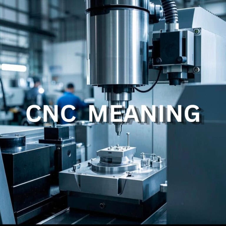
When wafers are transferred inside semiconductor equipment, the process may look simple, but the parts responsible for that movement face demanding requirements for precision, weight, surface condition, and operating stability. Components such as wafer handling arms, positioning bases, support parts, and clamping structures can affect equipment performance if even a small dimensional deviation occurs. Thin-wall, lightweight, and complex components are particularly challenging to manufacture with conventional methods. CNC machining uses digitally controlled tool paths and carefully selected materials and processes to help wafer handling parts achieve a better balance of dimensional accuracy, surface quality, and production consistency.
Why Do Wafer Handling Parts Require High-Precision CNC Machining?
Semiconductor equipment usually has limited internal space, while wafer handling components must operate repeatedly and maintain highly accurate positioning. A small deviation in a hole location or slight deformation of a component can affect assembly and motion accuracy. When sourcing these parts, manufacturers need to consider more than individual dimensions. Overall structure, weight, surface condition, and long-term dimensional stability are also important.
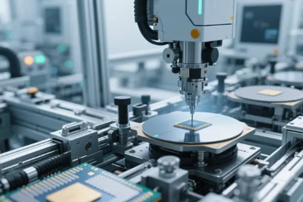
Small Structural Features Still Require Stable Accuracy
Wafer handling parts often include mounting holes, locating surfaces, connection structures, and motion-related mating areas. These features have close dimensional relationships, meaning that one dimension being within tolerance does not necessarily guarantee proper assembly.
Common machining requirements include:
- Stable mounting hole positions to prevent assembly misalignment.
- Accurate locating surface dimensions to maintain the correct reference relationship.
- Consistent dimensions in moving areas to reduce the risk of interference or unstable motion.
- High batch-to-batch consistency to minimize repeated equipment adjustment.
Precision CNC machining can reduce variations caused by manual operation through programmed tool control, allowing the same process to be repeated with stable results. For semiconductor wafer handling equipment, this consistency is often more valuable than simply pursuing extremely tight tolerances on a single dimension.
Thin-Wall and Lightweight Structures Are Difficult to Machine
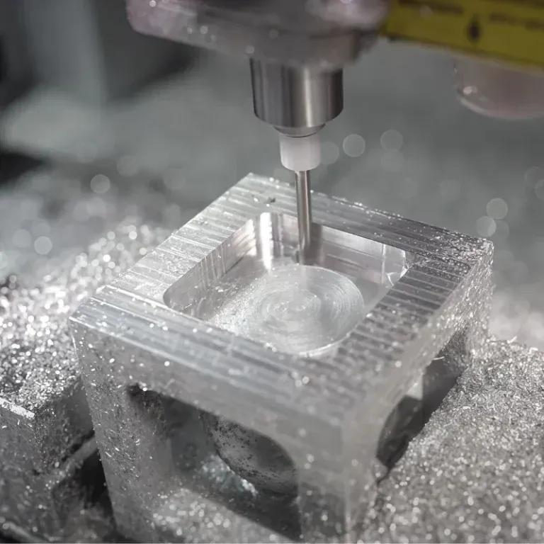
To reduce the moving load of wafer handling mechanisms, some components use thin-wall, hollow, or lightweight structures. However, removing more material can reduce structural rigidity. If cutting forces, clamping pressure, or machining sequences are not properly controlled, deformation may occur, eventually affecting assembly clearances and motion accuracy.
Different Materials Require Different Machining Methods
Wafer handling equipment may use aluminum alloys, stainless steel, engineering plastics, and other materials. Material properties directly affect tool selection, machining parameters, and surface treatment. Aluminum alloys require careful control of deformation and surface finish, stainless steel requires attention to tool wear and machining heat, while engineering plastics such as PEEK and POM require control of heat and dimensional changes caused by mechanical stress.
| Common Material | Applications in Wafer Handling Parts | CNC Machining Considerations |
| Aluminum Alloy | Robotic structures, supports, mounting components | Deformation, surface quality, hole position accuracy |
| Stainless Steel | Connectors, locating parts, corrosion-resistant structures | Tool wear, cutting heat, machining efficiency |
| PEEK | Insulating parts, chemically resistant components | Thermal deformation, dimensional stability |
| POM | Locating parts, sliding structures | Burrs, deformation, mating dimensions |
Once the material has been selected, the machining route should be adjusted accordingly. Wafer handling components cannot be manufactured simply by changing the cutting tool. Equipment condition, tool paths, fixturing, and inspection all need to work together.
What Needs to Be Controlled During CNC Machining of Wafer Handling Parts?
Once production begins, the main challenges usually involve deformation control, surface quality, and dimensional inspection. Thin-wall components and complex structures may appear normal during rough machining but develop dimensional changes during finishing. Including these risks in the process plan from the beginning makes production more stable.
Optimize Tool Paths to Reduce Deformation Risk
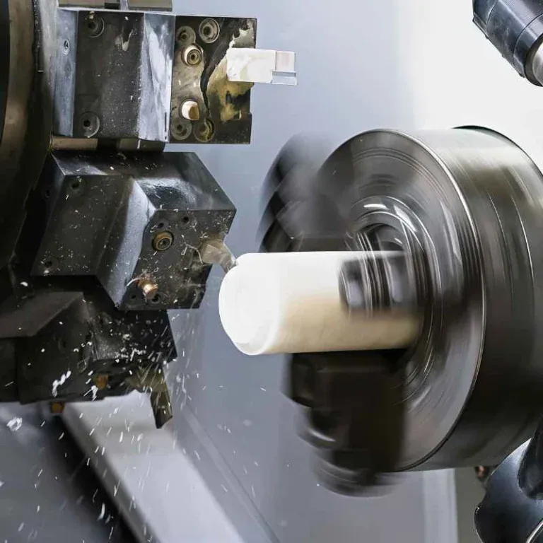
Wafer handling parts are generally not suitable for removing large amounts of material in a single operation, especially when they contain thin walls, deep cavities, or hollow structures. Proper sequencing of roughing, semi-finishing, and finishing operations can help control internal stress and reduce uneven loading on the part.
Key process controls include:
- Machining the overall profile first and gradually processing critical features.
- Leaving appropriate stock on thin-wall areas to avoid excessive cutting depth.
- Optimizing tool entry and exit paths to reduce sudden increases in cutting load.
- Using stable fixturing to prevent deformation caused by excessive clamping force.
For complex wafer handling components, tool path design should not focus only on machining speed. The goal is to maintain a stable relationship between the machine, cutting tool, and workpiece. A smoother machining process makes final finishing and dimensional inspection easier to control.
Surface Condition Cannot Be Judged by Appearance Alone
Although wafer handling components may not directly contact the wafer, their surface condition can still affect the internal equipment environment. Burrs, residual chips, and visible machining defects need to be removed or controlled, and some components may also require cleaning or surface treatment. For high-performance semiconductor equipment, visual inspection should only serve as an initial screening step and cannot replace dimensional or surface quality inspection.
Inspection Should Follow the Drawing Requirements
Different components require different inspection priorities. Mounting plates may focus on hole positions and flatness, robotic arm connectors may require closer control of critical axes and mating dimensions, while thin-wall structures require particular attention to deformation. Inspection procedures should follow actual assembly and application requirements rather than applying exactly the same inspection method to every component.
| Inspection Item | Key Inspection Content | Common Inspection Method |
| Dimensional Accuracy | Length, thickness, hole diameter, etc. | Calipers, micrometers, bore gauges |
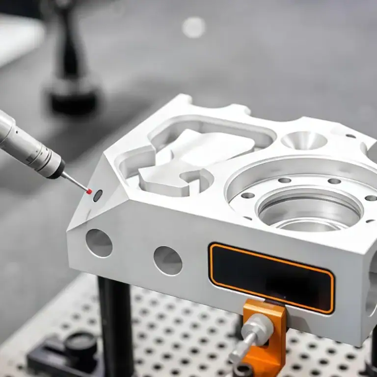
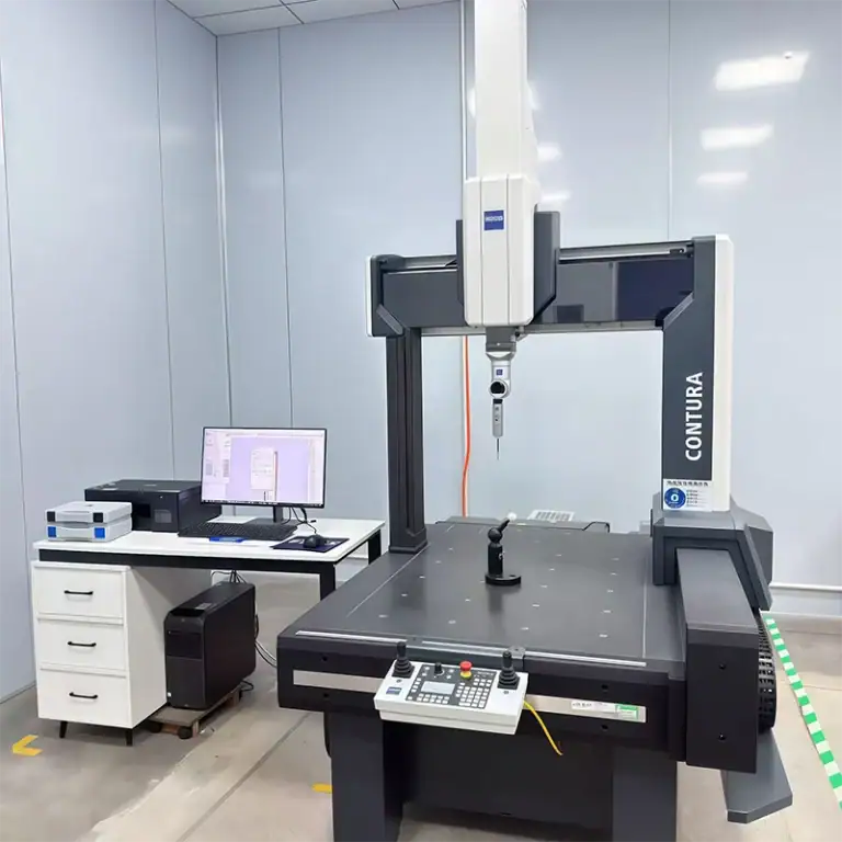
| Positional Accuracy | Hole positions, locating surfaces, axis relationships | Coordinate Measuring Machine (CMM) |
| Flatness | Flatness of mounting reference surfaces | Height gauge, CMM |
| Surface Roughness | Surface condition of mating and critical areas | Roughness tester |
| Visual Condition | Burrs, scratches, impact marks, etc. | Visual and magnified inspection |
Clear inspection data also makes production issues easier to trace. For semiconductor equipment components purchased over the long term, inspection records can help identify changes caused by tool wear, machine condition, and other manufacturing factors.
How Do You Choose a CNC Machining Supplier for Wafer Handling Parts?
Wafer handling components are highly customized precision parts, so procurement decisions should not be based on unit price alone. Machining experience, equipment stability, inspection capabilities, and response speed can all have a major impact on project progress. During semiconductor equipment development, drawings may change repeatedly, and a machining supplier that simply follows drawings without providing manufacturing feedback can create additional communication and development costs.
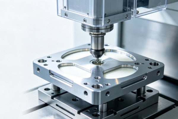
Check for Semiconductor Equipment Machining Experience
A machining team with semiconductor equipment experience is generally more familiar with thin-wall structures, lightweight designs, precision hole positions, and the practical challenges of engineering plastics. Experienced engineers can identify potential risks before production and adjust machining processes according to material and structural requirements instead of waiting until defects appear and rework becomes necessary.
Make Sure Equipment and Inspection Capabilities Match the Project
Equipment does not need to be the most advanced available. What matters is whether the available capabilities match the actual part requirements. A standard mounting plate and a complex thin-wall robotic arm require very different machining capabilities, while inspection equipment must also match the tolerances specified on the drawings.
When evaluating a supplier, it is useful to check:
- Whether stable CNC milling capabilities are available.
- Whether complex multi-surface structures can be machined with fewer setups.
- Whether aluminum alloys, stainless steel, and engineering plastics can be processed reliably.
- Whether precision inspection equipment such as CMMs is available.
Machining equipment is responsible for producing the part, while inspection equipment verifies whether the result meets the required specifications. For semiconductor equipment components, both manufacturing and quality verification capabilities need to be considered.
Lead Time and Engineering Response Speed Also Matter
Semiconductor equipment development often involves structural revisions, so manufacturers need more than one-time production support. The ability to quickly update CNC programs after drawing changes, provide timely feedback when prototype issues occur, and carry the same proven process into small-batch production can directly affect project schedules.
CNC machining of wafer handling parts is not simply about achieving small dimensions. It requires stable control of structural accuracy, thin-wall deformation, material characteristics, surface condition, and batch consistency. For semiconductor equipment manufacturers, a stable machining solution can reduce repeated adjustments and help components move more smoothly into assembly and testing. TIRAPID specializes in precision CNC machining services, supporting wafer handling parts and other customized precision components for semiconductor equipment.